Methods of forming through-substrate interconnects

A substrate and semiconductor technology, applied in semiconductor devices, electrical components, nanotechnology, etc.

Inactive Publication Date: 2009-12-02
HEWLETT PACKARD DEV CO LP
View PDF0 Cites 11 Cited by
  • Summary
  • Abstract
  • Description
  • Claims
  • Application Information

AI Technical Summary

Problems solved by technology

Therefore, an incompletely filled opening 156 cannot be reliably and reproducibly configured as figure 1 Shown are low-resistance through-substrate interconnects for electrically connecting active devices and / or passive components of semiconductor substrate 150 to another semiconductor stacked with semiconductor substrate 150 substrate and / or carrier substrate

Method used


Image

  • Methods of forming through-substrate interconnects
  • Methods of forming through-substrate interconnects
  • Methods of forming through-substrate interconnects

Examples


Embodiment Construction

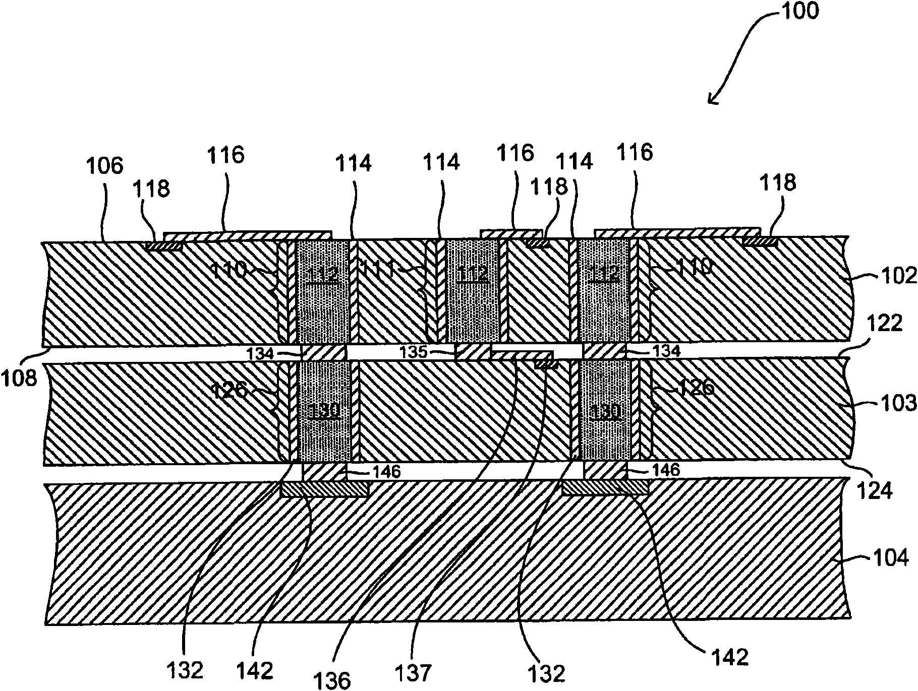
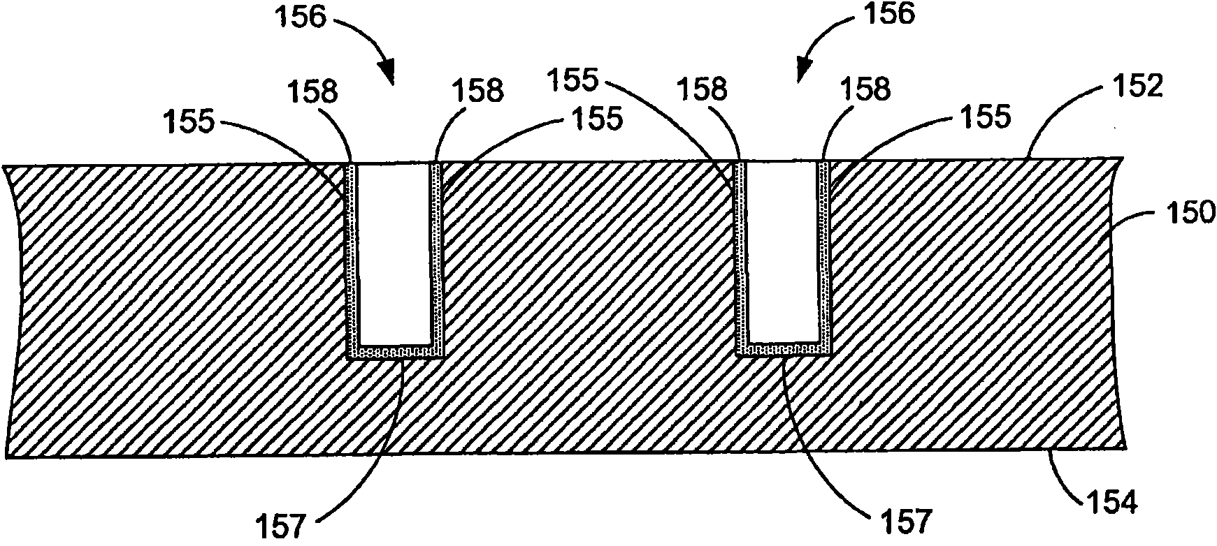
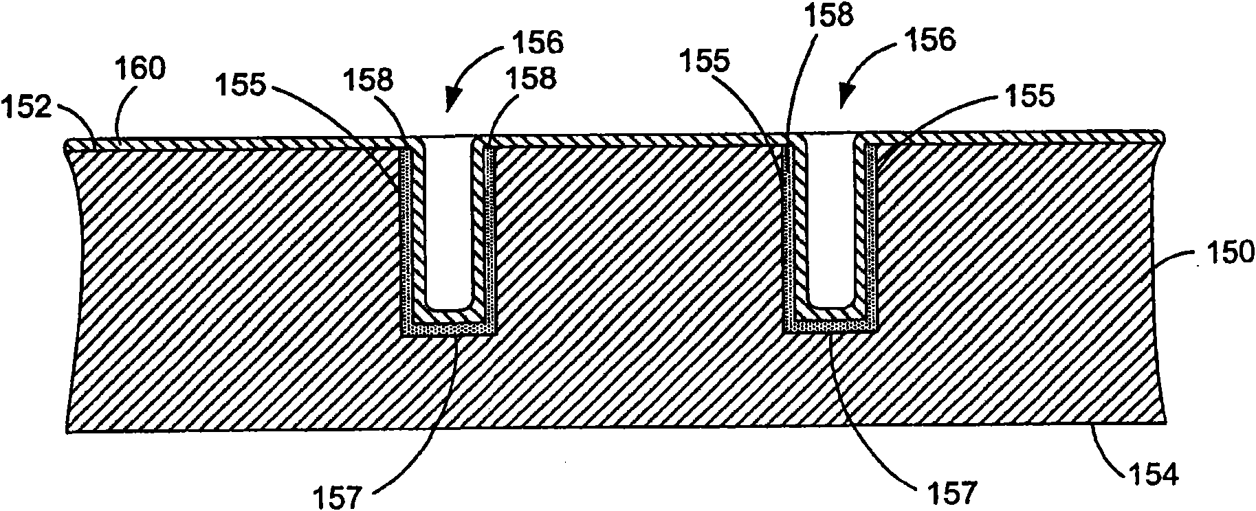
[0015] Various embodiments of the invention relate to methods of forming through-substrate interconnects. Figures 3A to 3K Illustrated is a method of forming at least one through-substrate interconnect according to an embodiment of the present invention, wherein at least one opening formed in a semiconductor substrate is filled with a conductive material grown in the presence of metal catalyst nanoparticles. Such as Figure 3A As shown, a semiconductor substrate 200 having an active face 202 and an opposite back face 204 is provided. The active face 202 includes a number of contact regions 206 (only two are shown for simplicity), each of which is electrically connected to an active semiconductor device (e.g., a transistor) and / or a passive element (e.g., a capacitor, resistor, or other passive components), the above-mentioned active semiconductor devices are located in the active region 208 formed under the active surface 202 , and the above-mentioned passive components can ...


PUM

PropertyMeasurementUnit
diameteraaaaaaaaaa

Abstract

In one embodiment of a method of forming at least one through-substrate interconnect, a semiconductor substrate (200) having first surface (202) and an opposing second substrate (204) is provided. At least one opening (210) is formed in the semiconductor substrate to extend from the first surface to an intermediate depth within the semiconductor substrate. The at least one opening is partially defined bya base (216). At least one metal-catalyst nanoparticle (220) is provided on the base. Conductive material is deposited within the at least one opening under conditiions in which the metal-catalyst nanoparticle promotes deposition of the conductive material (222). Material of the seminconductor substrate may be removed from the second surface to expose a portion of the conductive material filling the at least one opening (Figure 3K). In another embodiment, instead of using the nanoparticle, the conductive material may be selected to selectively deposit on the base partially defining the at least one opening.

Description

technical field [0001] Embodiments of the invention relate to semiconductor manufacturing. More particularly, embodiments of the invention relate to methods of forming through-substrate interconnects in a semiconductor substrate. Background technique [0002] Semiconductor devices including integrated circuits are mass-produced by fabricating hundreds or thousands of identical circuit patterns on a single semiconductor wafer or other semiconductor substrate using photolithography in combination with various other processes. In recent years, studies to increase the density of semiconductor devices in semiconductor assembly have increased. One technique for increasing the density of semiconductor devices in a semiconductor assembly is to stack multiple semiconductor substrates on top of each other. Forming through-substrate interconnects that penetrate semiconductor substrates to provide a conductive path from the active side of one semiconductor substrate to the backside of...

Claims


Application Information

Patent Timeline
Patent Type & Authority Applications(China)
IPC IPC(8): H01L21/768H01L21/28
CPCY10S977/89H01L2221/1094H01L21/76898Y10S977/892H01L24/82H01L2924/14H01L2924/00H01L21/768H01L21/28B82Y40/00
Inventor T·I·卡明斯
Owner HEWLETT PACKARD DEV CO LP
Why Eureka
Try Eureka