Functional molecular element, process for producing the same and functional molecular device

A molecular component and functional technology, applied in the field of functional molecular components, to achieve the effect of improving electrical interaction and reducing contact resistance

Inactive Publication Date: 2009-09-16
SONY CORP
View PDF4 Cites 1 Cited by
  • Summary
  • Abstract
  • Description
  • Claims
  • Application Information

AI Technical Summary

Problems solved by technology

[0030] However, the problem involved in the electrical connection through the connection between the thiol group and the gold electrode is that the molecule itself has electrical characteristics no matter how good, the connection part between its thiol terminal and the electrode has high resistance, and This high resistance limits the enhancement of molecular device properties (see, J.M.Wessels, H.G.Nothofer, W.E.Ford, F.von Wrochem, F.Scholz, T.Vossmeyer, A.Schroedter, H.Weller and A.Yasuda, "Optical and electrical properties of three-dimensional interlinked gold nanoparticle assemblies," Journal of the American Chemical Society, 126(10), 3349-3356, Mar 17, 2004)

Method used


Image

  • Functional molecular element, process for producing the same and functional molecular device
  • Functional molecular element, process for producing the same and functional molecular device
  • Functional molecular element, process for producing the same and functional molecular device

Examples


Embodiment approach 1

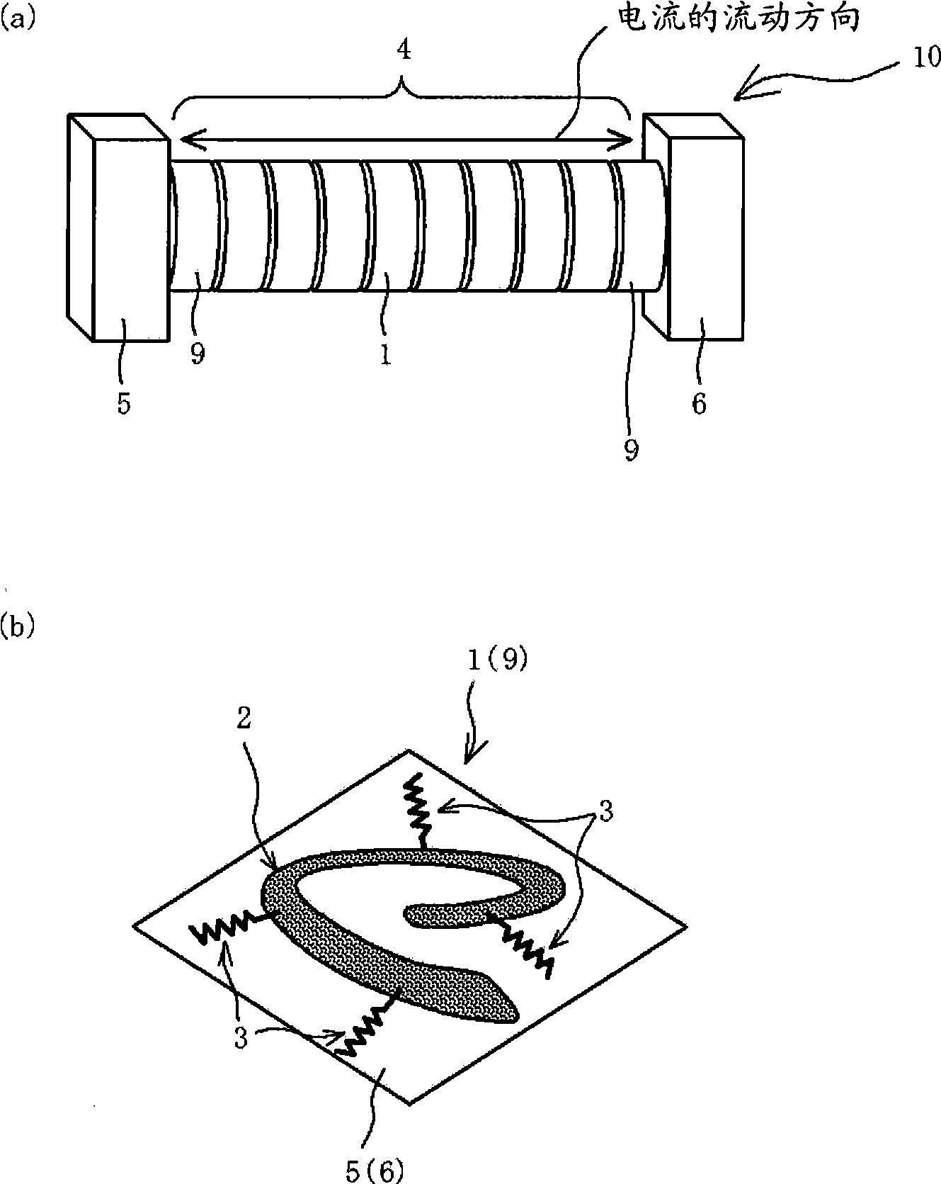
[0072] In Embodiment 1, examples of functional molecular elements mainly corresponding to claims 1 and 2 and claims 16 and 17 will be described.

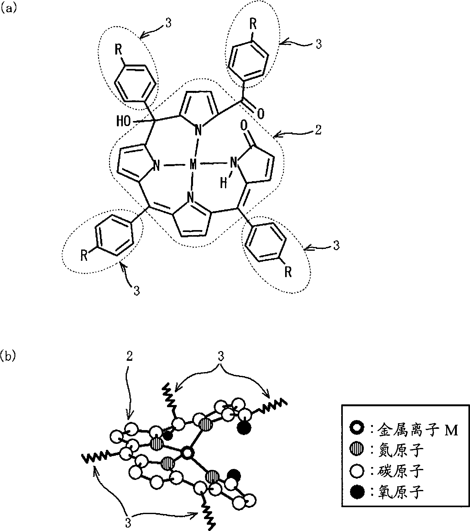
[0073] exist figure 2 In (a) of Embodiment 1, a structural formula of an example of the molecular structure of the π-electron conjugated molecule 1 constituting the above-mentioned array structure in Embodiment 1 is shown. exist figure 2 (b), schematically shown for the main showing figure 2 The π-electron conjugated molecule 1 shown in (a) of is substantially a three-dimensional structure of the disc-shaped skeleton portion 2 . exist figure 2 In (b) of , the metal ions M, nitrogen atoms, carbon atoms, and oxygen atoms constituting the skeleton portion 2 are shown as round spheres, while hydrogen atoms are omitted, and the side chain portion 3 is shown in a very simple omitted manner.

[0074] like figure 2 As shown in (a) and (b) of the π-electron conjugated molecule 1, the skeleton moiety 2 has biladienone (specifically,...

Embodiment approach 2

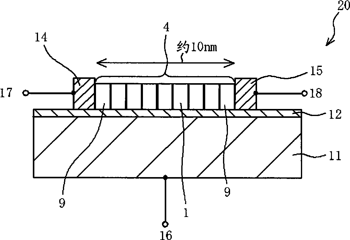
[0088] In Embodiment 2, as an example of a functional molecular device mainly corresponding to Claims 14 and 15, it will be described that the functional molecular element 10 described in Embodiment 1 above is formed between opposing electrodes and configured to be insulated Functional molecular devices for gate field effect transistors. image 3 It is a cross-sectional view for explaining the structure of the insulated gate field effect transistor 20 in the present embodiment.

[0089] like image 3 As shown, in the insulated gate field effect transistor 20, the doped silicon substrate 11 also serves as the gate electrode 13 as the above-mentioned control electrode. A silicon oxide layer as the gate insulating film 12 is formed on the surface of the silicon substrate 11 . The source electrode 14 and the drain electrode 15 made of gold are formed on, for example, a silicon oxide layer as the above-described counter electrodes, and the array structure 4 described in Embodimen...

Embodiment

[0097] Now, embodiments of the present invention will be described in detail below.

[0098]

[0099] exist Figure 4 In (a), a π-electron conjugated molecule 7 (corresponding to the above-mentioned π-electron conjugated molecule 1) having a substantially disc-shaped skeleton portion 2 used in the manufacture of the functional molecular element 10 in the present embodiment is shown 's structural formula. exist Figure 4 In (b) and (c) of , the structural formulas of 4-pentyl-4'-cyanobiphenyl (5CB) and tetrahydrofuran (THF) as solvents for producing the functional molecular element 10 are shown. The π-electron conjugated molecule 7 has a dodecyl-C attached to the para position 12 H 25 The phenyl group was used as the flexible side chain moiety of each of the zinc complexes of 3 dimethyl cholinone derivatives.

[0100] In order to correctly evaluate the properties of the functional molecular element 10, the functional molecular element 10 with good reproducibility should ...


PUM


Abstract

It is intended to provide a functional molecular element having a specific conductivity, which is a functional molecular element having a structure enabling reduction in the contact resistance at the interface between a constituting molecule and an electrode, a process for producing the same and a functional moleucalr device. A n-electron conjugated molecule (1), which is one species of linear tetrapyrrole having an almost disc-shaped central skeleton (2) and a flexible side chain (3) consisting of an alkyl group, is dissolved in 4-pentyl-4'-cyanobiphenyl or tetrahydrofuran and the concentration is adjusted to an appropriate level. This solution is adhered to electrodes (5) and (6) and the solvent is evaporated. Thus, an array structure (4) of the n-electron conjugated molecule (1) is self-organizingly formed. An adsorbed molecule (9) in the first layer of the array structure (4) is fixed in such a manner that its side chain (3) is adsorbed on the surface of the electrode (5) or (6) while the almost disc-shaped face of the sekeleton (2) is adhered in parallel to the surface of the electrode (5) or (6). The stacking direction of the n-electron conjugated molecule (1) in the second layer and thereafter of the array structure (4) is regulated by the n-n interaction between the disc-shaped face of the sekeletons (2).

Description

technical field [0001] The present invention relates to a functional molecular element with specific conductivity, its manufacturing method and functional molecular device. Background technique [0002] Nanotechnology is a method for observing, manufacturing and using -8 m = 10nm) fine structure technology. [0003] In the second half of the 1980s, an ultrahigh-precision microscope called a scanning tunneling microscope was invented, making it possible to see individual atoms and individual molecules. The use of scanning tunneling microscopes makes it possible not only to observe atoms and molecules, but to manipulate (manipulate) them one by one. [0004] For example, examples have been reported in which atoms are arranged on the surface of a crystal to draw characters and the like. Although it is possible to manipulate atoms and molecules, it is impractical to manufacture or assemble new materials or new devices by manipulating a large number of atoms or molecules one b...

Claims


Application Information

Patent Timeline
Patent Type & Authority Applications(China)
IPC IPC(8): H01L51/30H01L29/06H01L51/05
CPCB82Y10/00H01L51/0084H01L51/0595H01L51/0575H01L51/0092H01L51/0512H10K85/341H10K85/381H10K10/462H10K10/20H10K10/701H01L29/06H10K10/00
Inventor 松居惠理子琴昌大喜多浩二朗畠沢刚信
Owner SONY CORP
Why Eureka
Try Eureka