Memory circuit

A technology for storing circuits and voltages, applied in the field of memory arrays

Active Publication Date: 2009-08-26
TAIWAN SEMICON MFG CO LTD
View PDF3 Cites 7 Cited by
  • Summary
  • Abstract
  • Description
  • Claims
  • Application Information

AI Technical Summary

Problems solved by technology

The same problem occurs even in single-supply architectures operating below 1 volt

Method used


Image

  • Memory circuit
  • Memory circuit
  • Memory circuit

Examples


Embodiment Construction

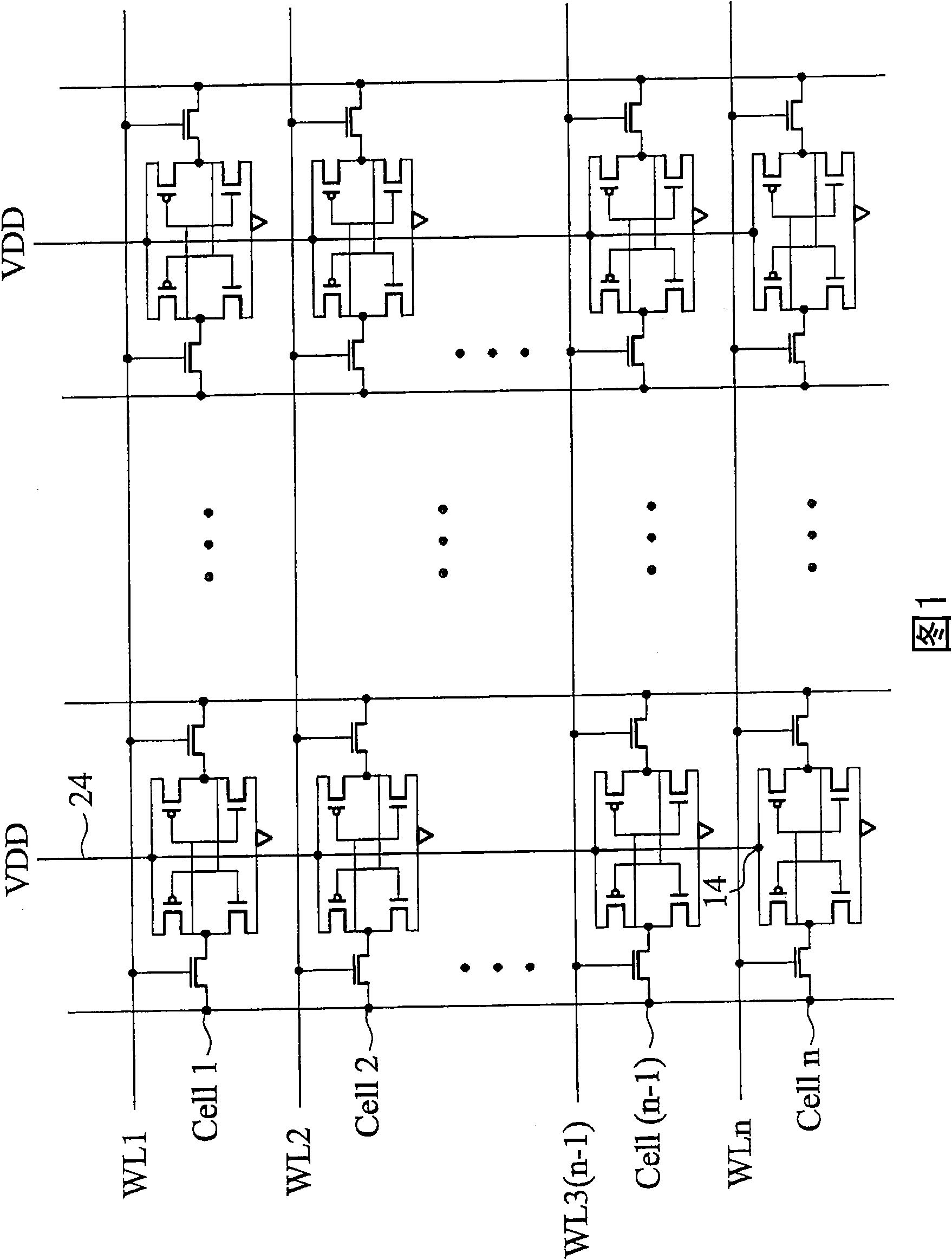
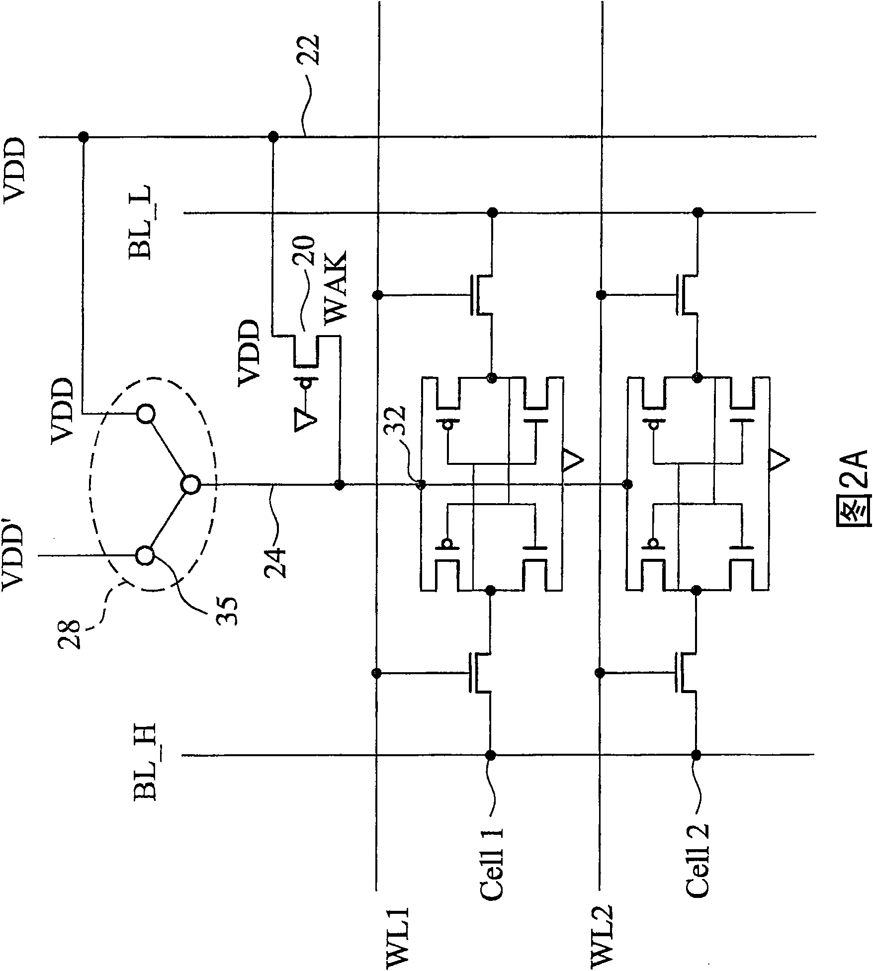
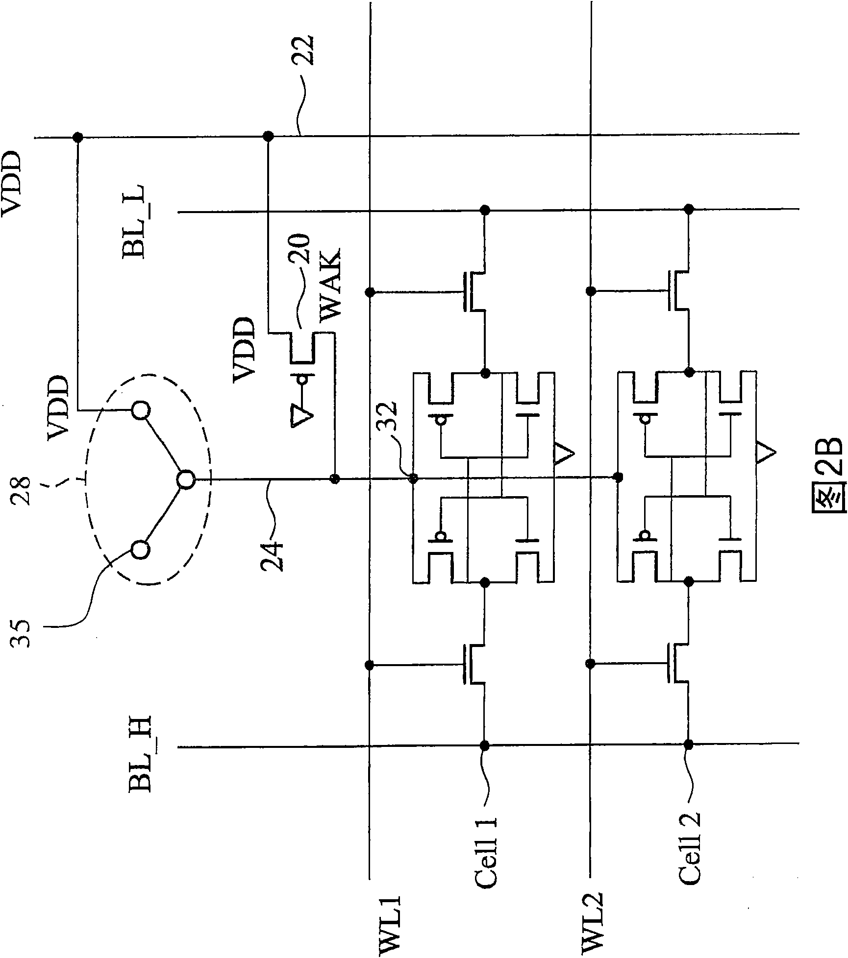
[0019] Figure 2A An example of the present invention is shown. The SRAM cells Cell1 and Cell2 form a pair and share a write-assist-keeper (WAK) device 20 . The SRAM cells Cell1 and Cell2 are respectively connected to word lines WL and WL', and share a pair of bit lines BL_H and BL_L. In the following figures, although each SRAM cell only includes 6 transistors (6T), however, the concept of the present invention can be easily applied to SRAM cells with different numbers of transistors (eg, 8T, 12T, etc.).

[0020] In a preferred embodiment, the WAK device 20 is a P-type metal oxide semiconductor (PMOS) transistor. In other embodiments, the WAK device can also be an N-type metal oxide semiconductor (NMOS) transistor, or other devices with a regulating current. In the best case, the WAK device is a conductor when the supply voltage is applied. Thus, in Figure 2A and Figure 2B In certain embodiments, the gate of the WAK device 20 is connected to VSS (or ground), or to ano...


PUM


Abstract

A memory circuit includes a bit line; a word line; a first power supply node having a first power supply voltage; a first power supply line connected to the first power supply node; a second power supply node selected from a group consisting of a floating node and a node having a second power supply voltage lower than the first power supply voltage; a second power supply line configured to switch connections between the first and the second power supply nodes; a write-assist-keeper (WAK) device coupling the first and the second power supply lines; and a static random access memory (SRAM) cell connected to the bit line, the word line and the second power supply line. The invention increases read voltage tolerance and write voltage tolerance, improves VCCMIN.

Description

technical field [0001] The present invention relates to memory arrays, in particular to static random access memory (Static Random Access Memory, SRAM) arrays. Background technique [0002] Static Random Access Memory (SRAM) is often used in integrated circuits. An important feature of the SRAM lattice is that it does not need to refresh the memory to maintain data. SRAM cells have several different transistors and are often named according to the number of transistors they have, for example: 6T SRAM with six transistors, 8T SRAM with eight transistors, and so on. Generally, the plurality of transistors function as data latches to store one bit. In addition, other transistors can be added on it to control its access. The plurality of SRAM cells are usually arranged in an array with rows and columns. Each row of the plurality of SRAM cells is connected to a word line, and the word line determines which SRAM cell will be selected. Each column of the plurality of SRAM cell...

Claims


Application Information

Patent Timeline
Patent Type & Authority Applications(China)
IPC IPC(8): G11C11/41G11C11/413
CPCG11C11/419G11C11/417G11C5/147
Inventor 苏布拉曼·坎葛利巴拉斯·乌普杜利
Owner TAIWAN SEMICON MFG CO LTD
Why Eureka
Try Eureka