


Quick Research
Generate reliable direction feasibility study reports for your R&D in just a few steps.

Technical Q&A
Discover and master advanced knowledge NOW. Basics, ideas, possibilities, all at once.

Find Solutions
As an expert in R&D theories, this can generate solutions to your technical problems instantly.

Evaluate Feasibility
Analyze your overall solution with one click, know your potential R&D risks in advance.

Monitor Landscape
Get weekly tech updates, stay abreast of the latest tech innovations and key insights.
Amplifier circuit and display apparatus having the same
A technology for amplifying circuits and amplifying parts, applied in the direction of negative feedback circuit layout, static indicators, instruments, etc., to achieve the effects of preventing errors, improving stability and low power consumption, and reducing power consumption
- Summary
- Abstract
- Description
- Claims
- Application Information
AI Technical Summary
Problems solved by technology
Method used
Image

Examples
no. 1 Embodiment approach
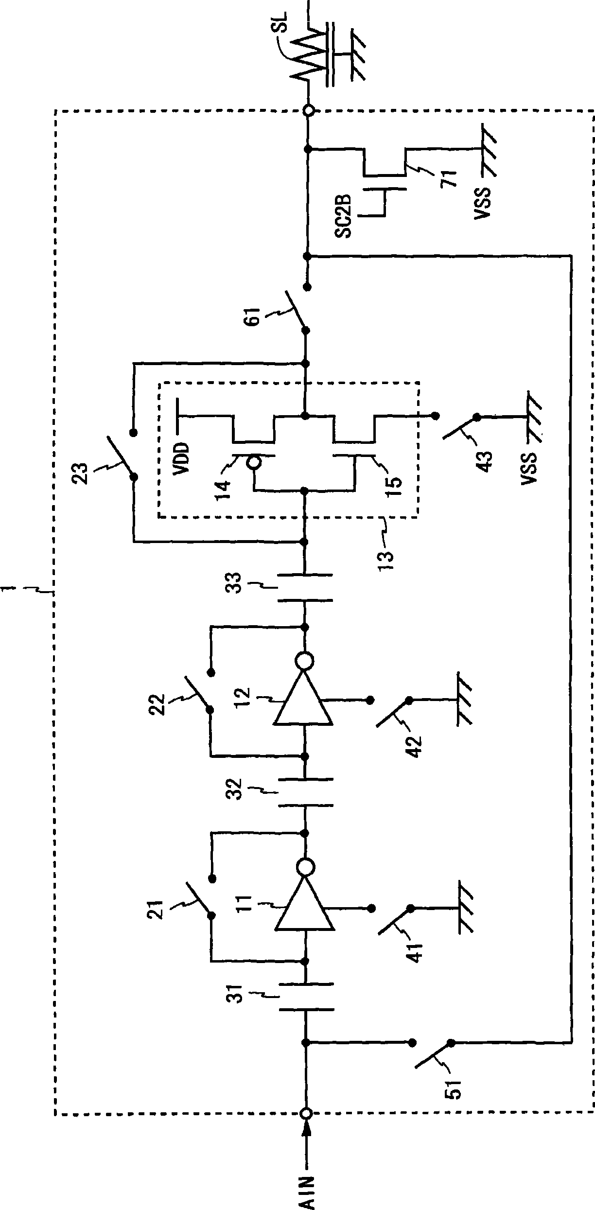
[0127] figure 1 It is a circuit diagram of an amplifier circuit according to the first embodiment of the present invention. figure 1 In the amplifying circuit 1 shown, a plurality of amplifiers (inverters) connected in cascade are used to amplify the analog input signal AIN, and the amplified signal is used to drive the signal line SL (details will be described later). The amplifier circuit 1 is used, for example, when driving data signal lines of a liquid crystal display device.
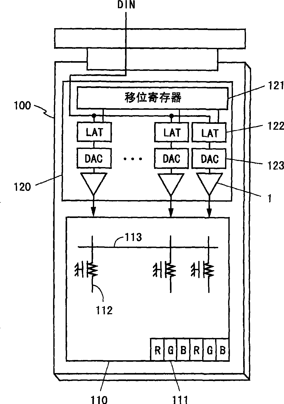
[0128] figure 2 It is a block diagram showing the configuration of a liquid crystal display device having an amplifier circuit 1 . figure 2In the illustrated liquid crystal display device, a pixel array 110 , a data signal line driver circuit 120 , and a scanning signal line driver circuit (not shown) are integrally formed on a liquid crystal panel 100 . The pixel array 110 includes a plurality of pixel circuits 111 arranged two-dimensionally, a plurality of data signal lines 112 , and a plural...
no. 2 Embodiment approach
[0166] Figure 10 It is a circuit diagram of an amplifier circuit according to a second embodiment of the present invention. Figure 10 The amplifier circuit 2 shown is the amplifier circuit 1 according to the first embodiment ( figure 1 ), the inverter 13 is replaced by the inverter 16 (including the separation switch 62), and the separation switch 61 and the capacitor 33 are removed. The amplifying circuit 2 is the same as the amplifying circuit 1, and can be used when driving a data signal line of a liquid crystal display device (refer to figure 2 and image 3 ). Among the constituent elements of the present embodiment, the same reference numerals are assigned to the same elements as those of the first embodiment, and description thereof will be omitted.
[0167] In the amplifier circuit 2, switches 21 and 22 functioning as threshold value setting switches are provided corresponding to the respective inverters 11 and 12 other than the final stage. In addition, a capac...
no. 3 Embodiment approach
[0175] Figure 12 It is a circuit diagram of an amplifier circuit according to a third embodiment of the present invention. Figure 12 The amplifier circuit 4 shown is the amplifier circuit 2 according to the second embodiment ( Figure 10 ) is obtained by adding a capacitor 34. The amplifying circuit 4 is the same as the amplifying circuit 1, and can be used when driving the data signal lines of the liquid crystal display device (refer to figure 2 and image 3 ). Among the constituent elements of the present embodiment, the same elements as those in the first or second embodiment are assigned the same reference numerals and description thereof will be omitted.
[0176] One electrode of the capacitor 34 is connected to the input terminal of the inverter 11 and supplies the low-level power supply voltage VSS to the other electrode of the capacitor 34 . The capacitor 34 functions as an input capacitive element, one electrode of which is connected to the input terminal of t...
PUM
 Abstract
Description
Claims
Application Information
 - R&D Engineer
- R&D Manager
- IP Professional
- Industry Leading Data Capabilities
- Powerful AI technology
- Patent DNA Extraction
Browse by: Latest US Patents, China's latest patents, Technical Efficacy Thesaurus, Application Domain, Technology Topic, Popular Technical Reports.
© 2024 PatSnap. All rights reserved.Legal|Privacy policy|Modern Slavery Act Transparency Statement|Sitemap|About US| Contact US: help@patsnap.com