Cooling type multi-punch semiconductor packaging construction

A heat-dissipating, semi-conductive technology, applied in the direction of semiconductor devices, semiconductor/solid-state device components, electric solid-state devices, etc., can solve problems such as heat sink offset, chip internal stress sealant thermal resistance, etc., to prevent peeling and increase stress Cushioning effect, the effect of improving heat dissipation effect

Inactive Publication Date: 2010-10-27
POWERTECH TECHNOLOGY
View PDF4 Cites 0 Cited by
  • Summary
  • Abstract
  • Description
  • Claims
  • Application Information

AI Technical Summary

Problems solved by technology

[0006] Another object of the present invention is to provide a novel heat dissipation type multi-perforated semiconductor packaging structure, the technical problem to be solved is to make it able to solve the problems of heat sink deviation, chip internal stress and sealing glue caused by the existing built-in heat sink The problem of thermal resistance, so it is more suitable for practical

Method used


Image

  • Cooling type multi-punch semiconductor packaging construction
  • Cooling type multi-punch semiconductor packaging construction
  • Cooling type multi-punch semiconductor packaging construction

Examples


no. 1 Embodiment

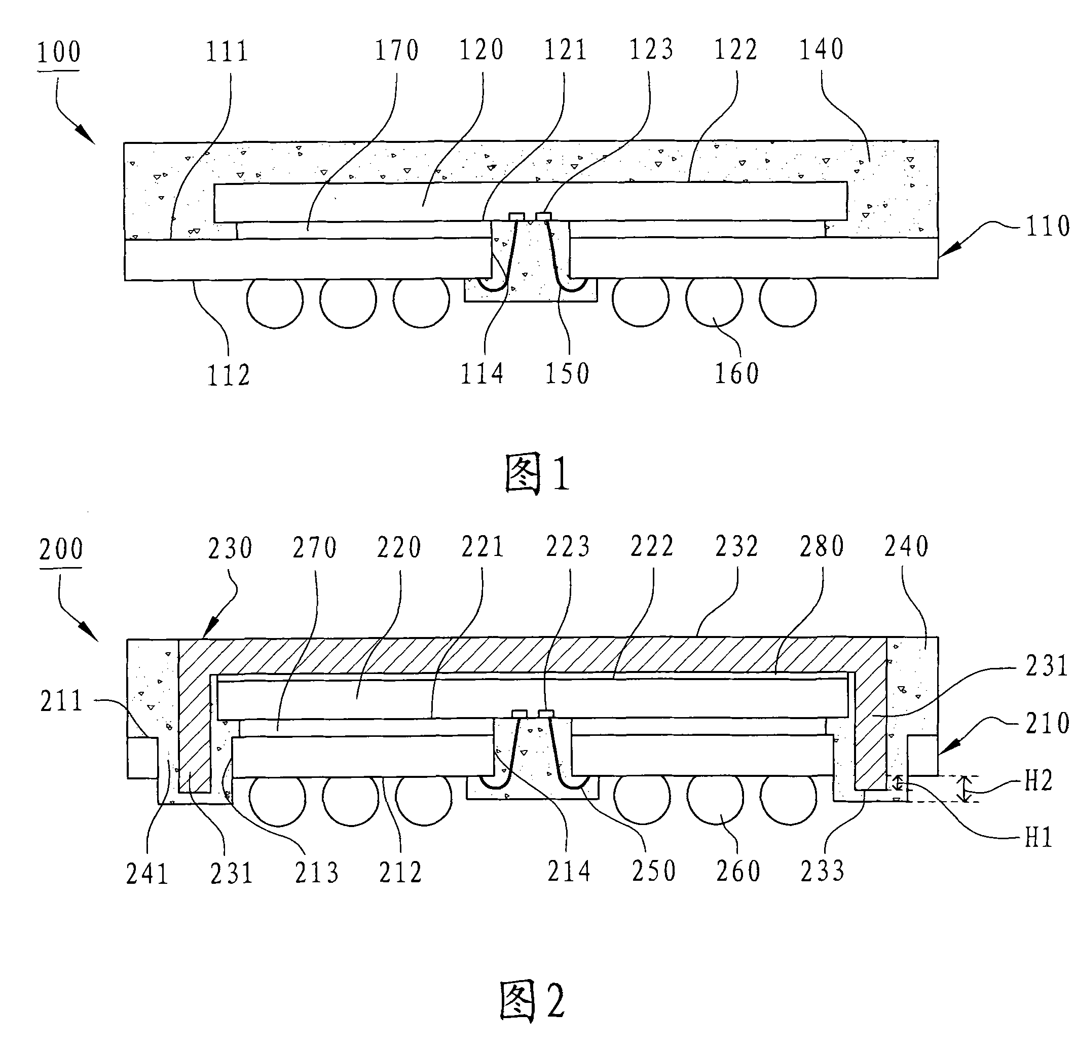
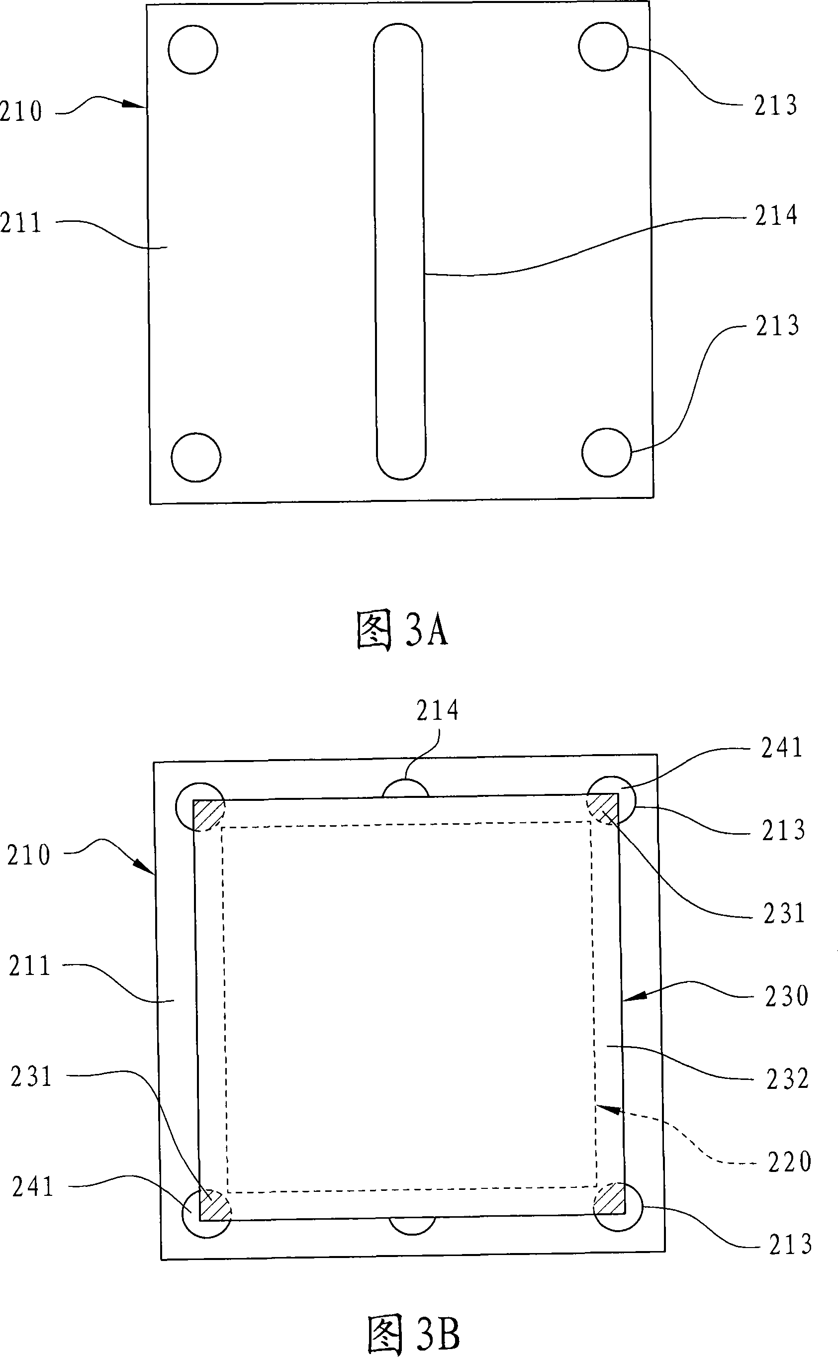
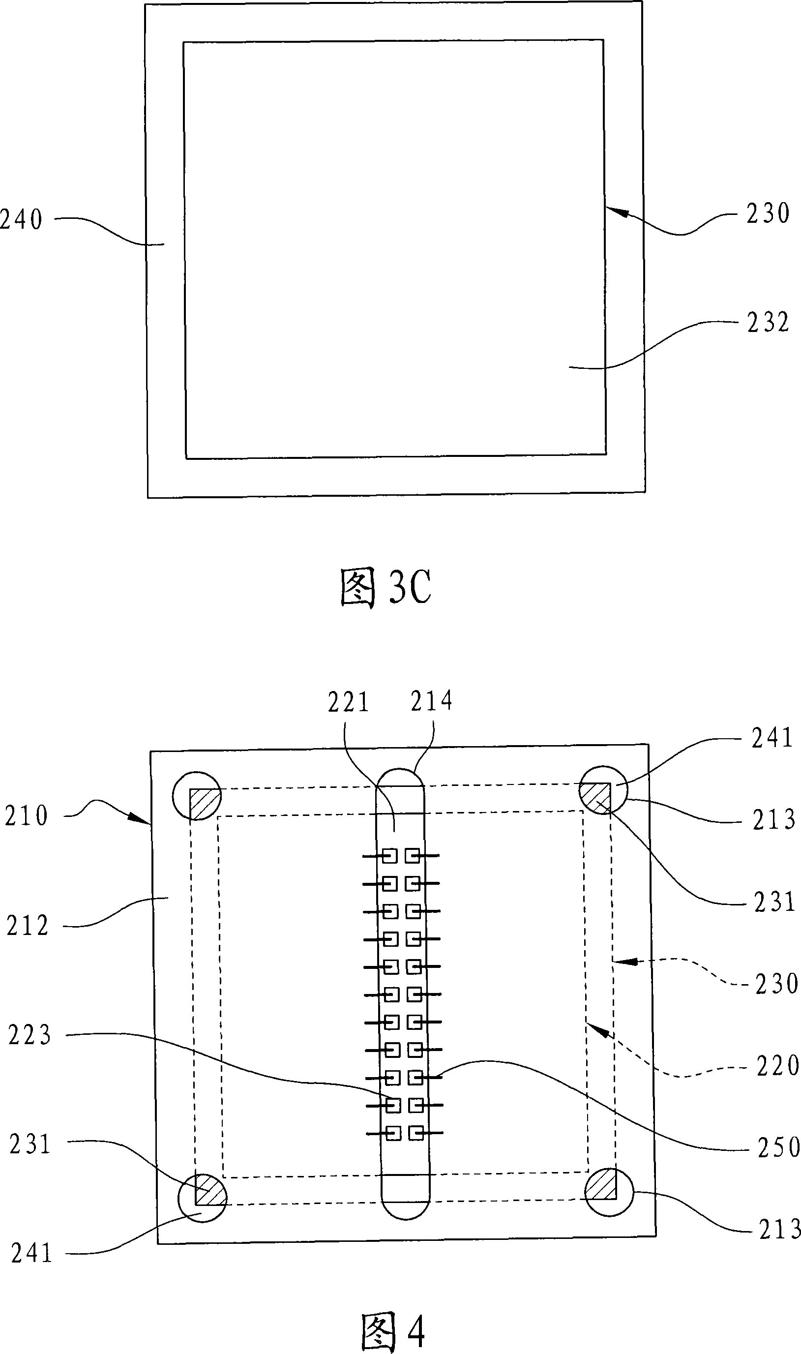
[0075] According to a first embodiment of the present invention, a heat dissipation type multi-through-hole semiconductor package structure is disclosed. see figure 2 As shown, a heat dissipation semiconductor package structure 200 with multiple through holes mainly includes a substrate 210 , a chip 220 , a built-in heat sink 230 and an encapsulant 240 . The substrate 210 has an upper surface 211 , a lower surface 212 and a plurality of positioning through holes 213 , and the positioning through holes 213 penetrate from the upper surface 211 to the lower surface 212 . In this embodiment, the positioning through holes 213 may include four corner through holes, which are adjacent to the four corners of the substrate 210 (such as Figure 3A shown). The substrate 210 may further have a slot 214 located on a central line of the substrate 210 and passing through the substrate 210 for passage of a plurality of electrical connection elements 250 in a subsequent electrical connectio...


PUM


Abstract

The invention relates to a cooling-typed multi-perforated semiconductor packaging structure, mainly comprising a substrate which has a plurality of positioning through-holes, a wafer which is arranged on the substrate, a built-in type cooling fin which is attached to the wafer, and an adhesive body; wherein, the built-in type cooling fin has a plurality of support legs and a cooling surface; and the support legs are inserted in the positioning through-holes which are also not fully filled by the support legs so as to provide a plurality of mold flow channels for covering the support legs. Therefore, the built-in type cooling fin can be positioned on the substrate under the condition of small amount of or no adhesive, and can be combined with the wafer and the substrate into a whole.

Description

technical field [0001] The invention relates to a semiconductor device, in particular to a heat dissipation type multi-through-hole semiconductor packaging structure. Background technique [0002] Usually, the chip is disposed on the substrate and the encapsulant is used to seal the chip to prevent the chip from being polluted by external pollutants. With the advancement of semiconductor packaging technology and the continuous improvement of chip circuit functions, the calculation speed of the chip is getting faster and faster, which will increase the temperature of the chip. Although the surface of these components (such as chip and encapsulant) has the effect of heat dissipation, the chip with higher frequency or power will relatively generate more heat during operation. If only the heat dissipation effect of the component itself is not enough Transfer the thermal energy generated by the wafer. Therefore, when the heat energy generated by the chip cannot be transferred t...

Claims


Application Information

Patent Timeline
Patent Type & Authority Patents(China)
IPC IPC(8): H01L23/367H01L23/31H01L23/13
CPCH01L2924/15311H01L2224/4824
Inventor 余秉勋洪菁蔚
Owner POWERTECH TECHNOLOGY
Why Eureka
Try Eureka