CMOS device metal grid and method for forming same

A metal gate and metal gate material technology, which is applied in the field of CMOS devices, can solve the problems of inability to meet the threshold voltage of nano-CMOS devices, complicated processes, and poor results, so as to overcome the problem of complex pattern etching, simplify the processing flow, reduce Effects of the deposition process

Inactive Publication Date: 2009-07-29
INST OF MICROELECTRONICS CHINESE ACAD OF SCI
View PDF0 Cites 11 Cited by
  • Summary
  • Abstract
  • Description
  • Claims
  • Application Information

AI Technical Summary

Problems solved by technology

However, the current method of adjusting the effective work function through these process factors is not effective, and the process is complicated, so the formed CMOS devices cannot meet the threshold voltage requirements of nano-CMOS devices

Method used


Image

  • CMOS device metal grid and method for forming same
  • CMOS device metal grid and method for forming same
  • CMOS device metal grid and method for forming same

Examples


Embodiment Construction

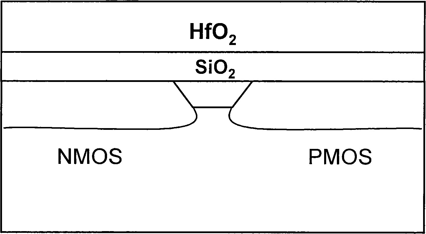
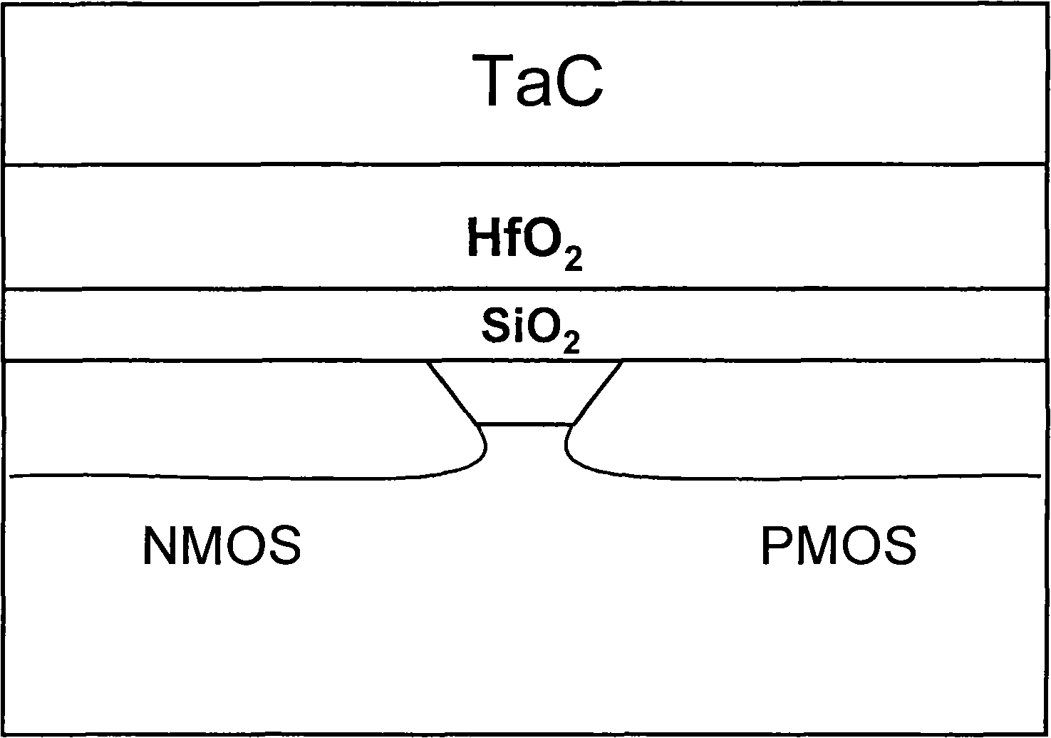
[0028] According to the technical solution provided by the present invention, by changing the film thickness of the metal gate of the CMOS device, the effective work function of the metal gate material at the same high-k can be significantly changed, thereby realizing the effective work function in a simple and effective manner. And the adjustment of the threshold voltage of the CMOS device, so that the formed CMOS device can meet the requirement of the threshold voltage of the nanometer CMOS device.

[0029] In order to make the object, technical solution and advantages of the present invention clearer, the present invention will be further described in detail below in conjunction with the accompanying drawings.

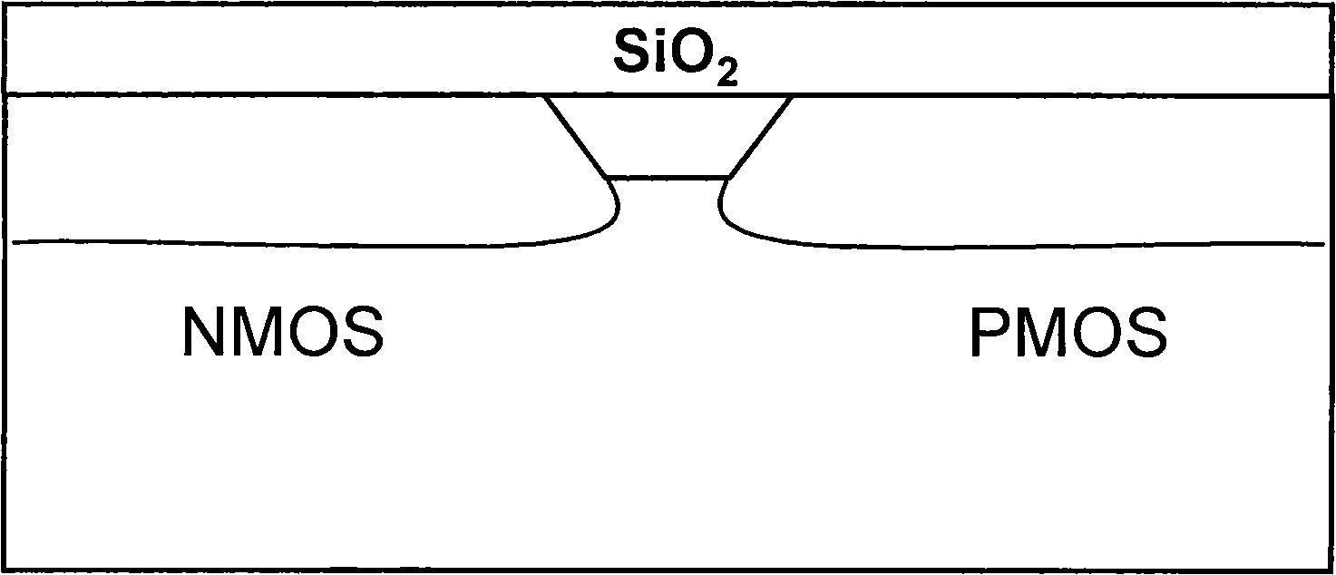
[0030] In the first embodiment of the present invention, as Figure 1-7 As shown, a non-limiting example thereof illustrates a technical solution for forming a metal gate structure of a CMOS device. details as follows:

[0031] Step 101: if figure 1 As shown, an...


PUM


Abstract

The invention provides a metal grid electrode of a CMOS element and a forming method thereof. With the technical proposal, the change of the thickness of the metal grid electrode can lead to obvious change of an effective work function value of the metal grid electrode material on the same high k (dielectric constant) grid medium, thus realizing the regulation of the effective work function value in simple and effective ways and further effectively regulating a threshold voltage of the high k grid medium / a CMOS element of a metal grid electrode structure. Therefore, the high k grid medium / the CMOS element of the metal grid electrode structure meeting the threshold voltage demands of a nano CMOS element can be obtained. Moreover, the adoption of the technical proposal can simplify the processing flow of the high k grid medium / the CMOS element of the metal grid electrode structure, thus not only reducing the deposition process of a double metal grid thin film, but also overcoming complex pattern etching problems of a double metal grid structure.

Description

technical field [0001] The present invention relates to the field of CMOS (Complementary Metal Oxide Semiconductor) devices in microelectronics technology, and more particularly relates to a metal gate of a CMOS device and a method for forming the same. Background technique [0002] With the rapid development of microelectronics technology, CMOS technology, the core of microelectronics technology, has become the supporting technology in modern electronic products. For decades, logic chipmakers have used silicon dioxide (SiO 2 ) as the gate dielectric and heavily doped polysilicon (poly-Si) as the gate electrode material. This combination continued into the 90nm technology generation. SiO in CMOS transistors as feature sizes continue to shrink 2 The size of the gate dielectric is approaching the limit, for example, in the 65nm process, SiO 2 The thickness of the gate has been reduced to 1.2 nanometers, which is about 5 silicon atomic layers thick. If it is further reduced...

Claims


Application Information

Patent Timeline
Patent Type & Authority Applications(China)
IPC IPC(8): H01L29/423H01L21/283H01L21/3213H01L27/092H01L21/8238
Inventor 王文武陈世杰陈大鹏
Owner INST OF MICROELECTRONICS CHINESE ACAD OF SCI
Why Eureka
Try Eureka