Nano lens and scanning microscope using the same
A lens, nanotechnology, applied in the field of scanning microscope
- Summary
- Abstract
- Description
- Claims
- Application Information
AI Technical Summary
Problems solved by technology
Method used
Image
Examples
Embodiment Construction
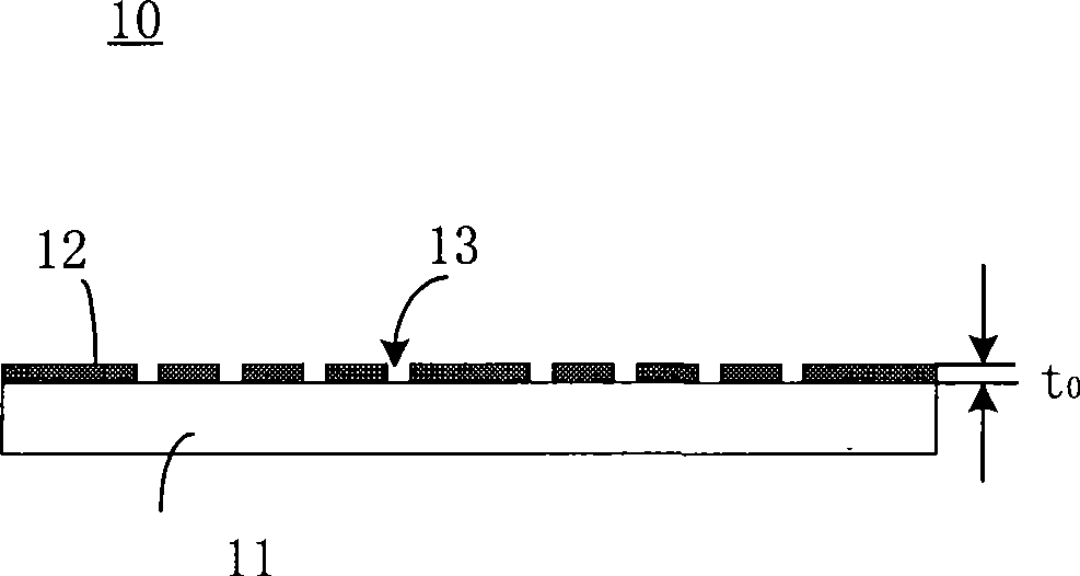
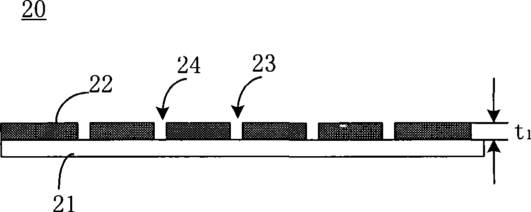
[0029] The nano lens consists of a substrate and a metal film deposited on the substrate. The substrate should be able to transmit the used light or electromagnetic waves (including microwave, millimeter wave, near-infrared, infrared, visible light, ultraviolet light, etc.), and may be quartz, plastic, etc. There are several nano-sized holes or concentric rings in the metal film. Among them, the diameter and distance of the small hole or ring of the film thickness must meet certain conditions. The present invention will be further described below in conjunction with several specific embodiments.
[0030] Figure 1A with Figure 1B It is a schematic diagram of the nano lens structure of the first embodiment of the present invention. As shown in the figure, the bottom layer of the nano lens 10 is a transparent substrate 11, for example, a glass sheet. There is a layer of opaque metal film 12 on the substrate, and the metal film 12 is formed by, for example, an evaporation process. ...
PUM
 Abstract
Description
Claims
Application Information
 - R&D
- Intellectual Property
- Life Sciences
- Materials
- Tech Scout
- Unparalleled Data Quality
- Higher Quality Content
- 60% Fewer Hallucinations
Browse by: Latest US Patents, China's latest patents, Technical Efficacy Thesaurus, Application Domain, Technology Topic, Popular Technical Reports.
© 2025 PatSnap. All rights reserved.Legal|Privacy policy|Modern Slavery Act Transparency Statement|Sitemap|About US| Contact US: help@patsnap.com


