High-brightness LED construction

A light-emitting diode, high-brightness technology, applied in the direction of electrical components, circuits, semiconductor devices, etc., can solve the problem of reducing luminous efficiency and achieve the effect of improving luminous efficiency

Inactive Publication Date: 2009-06-10
TEKCORE CO LTD
View PDF1 Cites 4 Cited by
  • Summary
  • Abstract
  • Description
  • Claims
  • Application Information

AI Technical Summary

Problems solved by technology

[0006] Although the above structure makes the current evenly distributed to achieve high-quality AlGaInP light-emitting diodes, because the light generated by the AlGaInP active layer 12 will be shielded by the front electrode 16, reducing the luminous efficiency

Method used


Image

  • High-brightness LED construction
  • High-brightness LED construction

Examples


Embodiment Construction

[0013] The detailed content and technical description of the present invention will be further described by examples, but it should be understood that these examples are for illustrative purposes only, and should not be construed as limitations on the implementation of the present invention.

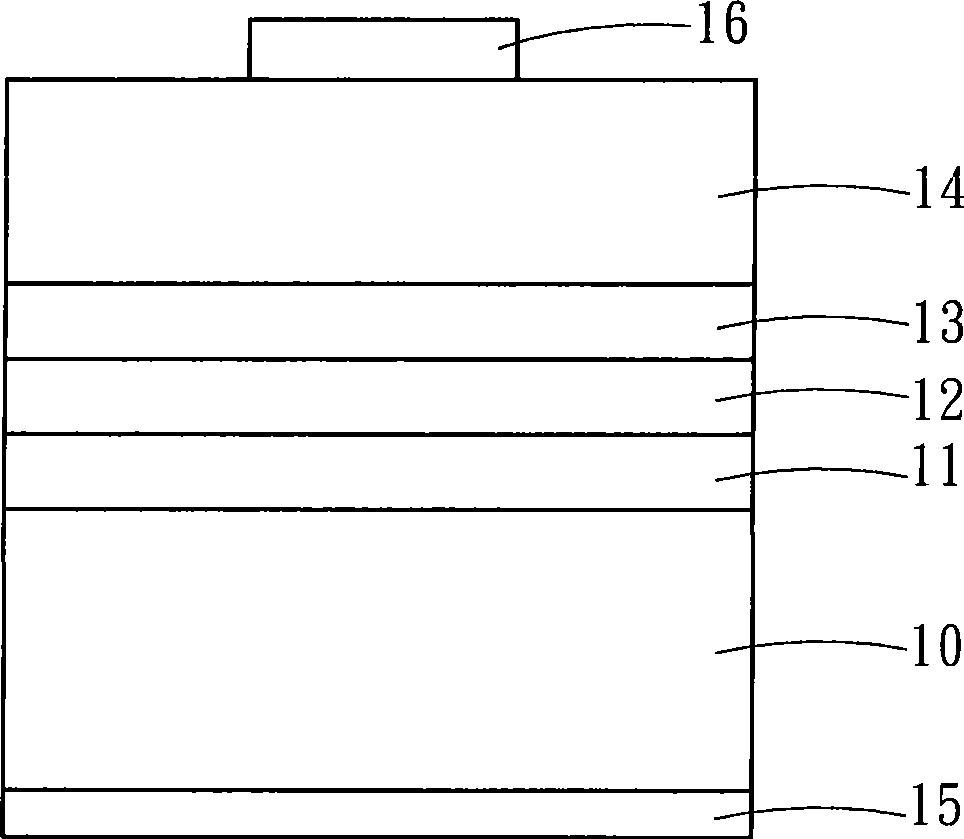
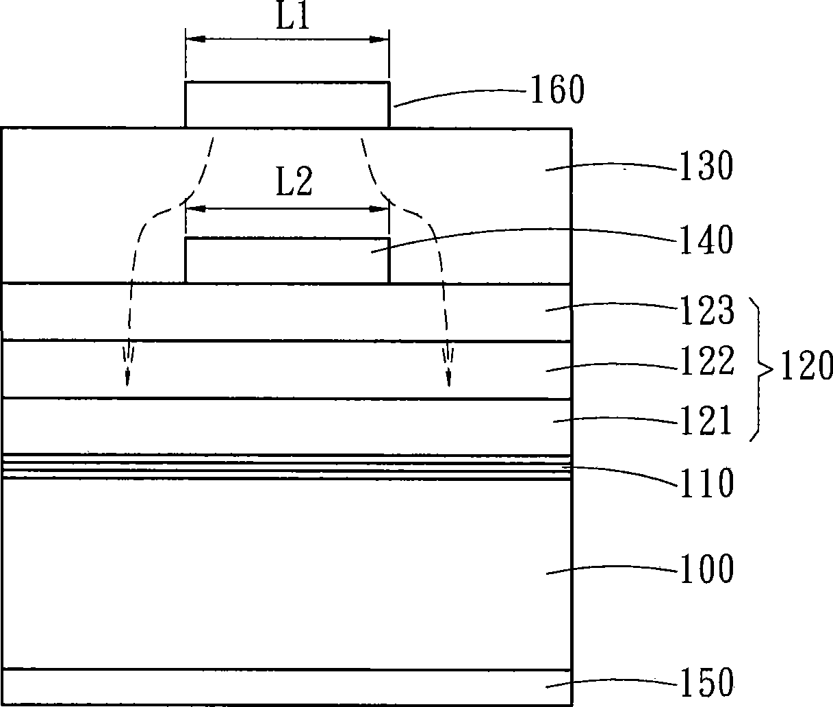
[0014] see figure 2 , the present invention proposes a high-brightness light-emitting diode structure, which at least includes: an n-type substrate 100 formed of gallium arsenide (GaAs), and an ohmic n-electrode 150 formed on the bottom surface thereof. A distributed Bragg reflection layer 110, the distributed Bragg reflection layer 110 is formed on the n-type substrate 100; the distributed Bragg reflection layer 110 can generally be made of Al x Ga 1-x As / Al y Ga 1-y Made of As material, where 0≦x≦1, 0≦y≦1, and x≠y.

[0015] An aluminum gallium indium phosphide (AlGaInP) semiconductor stack structure 120 is formed on the distributed Bragg reflection layer 110 for generating light i...


PUM

PropertyMeasurementUnit
Thicknessaaaaaaaaaa

Abstract

The invention relates to a high-brightness LED structure. A highly doped island structure layer formed by n-type aluminium phosphide indium (AlInP) is utilized to be formed on partial surface of a semiconductor laminated structure of aluminium phosphide gallium indium (AlGaInP) so as to form a current barrier. As the island structure layer is coated with a p-type window layer and is positioned below an ohm p electrode, strengthened input current flows to the semiconductor laminated structure of the AlGaInP, which is masked with a non-light-emitting surface electrode, so as to enable current distribution to reach an optimum state and then improve the light emitting efficiency of an LED.

Description

technical field [0001] The invention relates to a high-brightness light-emitting diode structure, which uses n-type aluminum indium phosphide as a current blocking structure to strengthen the input current to flow to the aluminum gallium indium phosphide semiconductor laminated area covered by the electrode on the non-light-emitting surface, thereby Make the current distribution reach the best state, and then improve the luminous efficiency. Background technique [0002] The basic principle of a light emitting diode (Light Emitting Diode, LED) is to generate light through the combination of electrons and holes. As far as the PN junction is concerned, when it is forward biased, electrons and holes are respectively injected into the depletion region (depletion region) , these injected electrons combine with holes, and their energy is emitted in the form of light. [0003] And since the rapid development of metal-organic chemical vapor deposition system (Metal-Organic Chemical...

Claims


Application Information

Patent Timeline
IPC IPC(8): H01L33/00H01L33/14H01L33/30
Inventor 郑香平杨昌义吴厚润
Owner TEKCORE CO LTD
Why Eureka
Try Eureka