Processing container an plasma processing device
A technology for processing containers and plasma, which is applied in the fields of plasma, semiconductor/solid-state device manufacturing, discharge tubes, etc., can solve problems such as heavy burden and increased component consumption, and achieve the effect of reducing costs and facilitating replacement operations.
- Summary
- Abstract
- Description
- Claims
- Application Information
AI Technical Summary
Problems solved by technology
Method used
Image
Examples
no. 1 approach
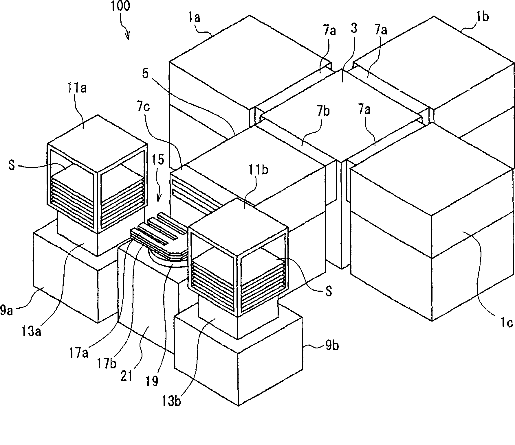
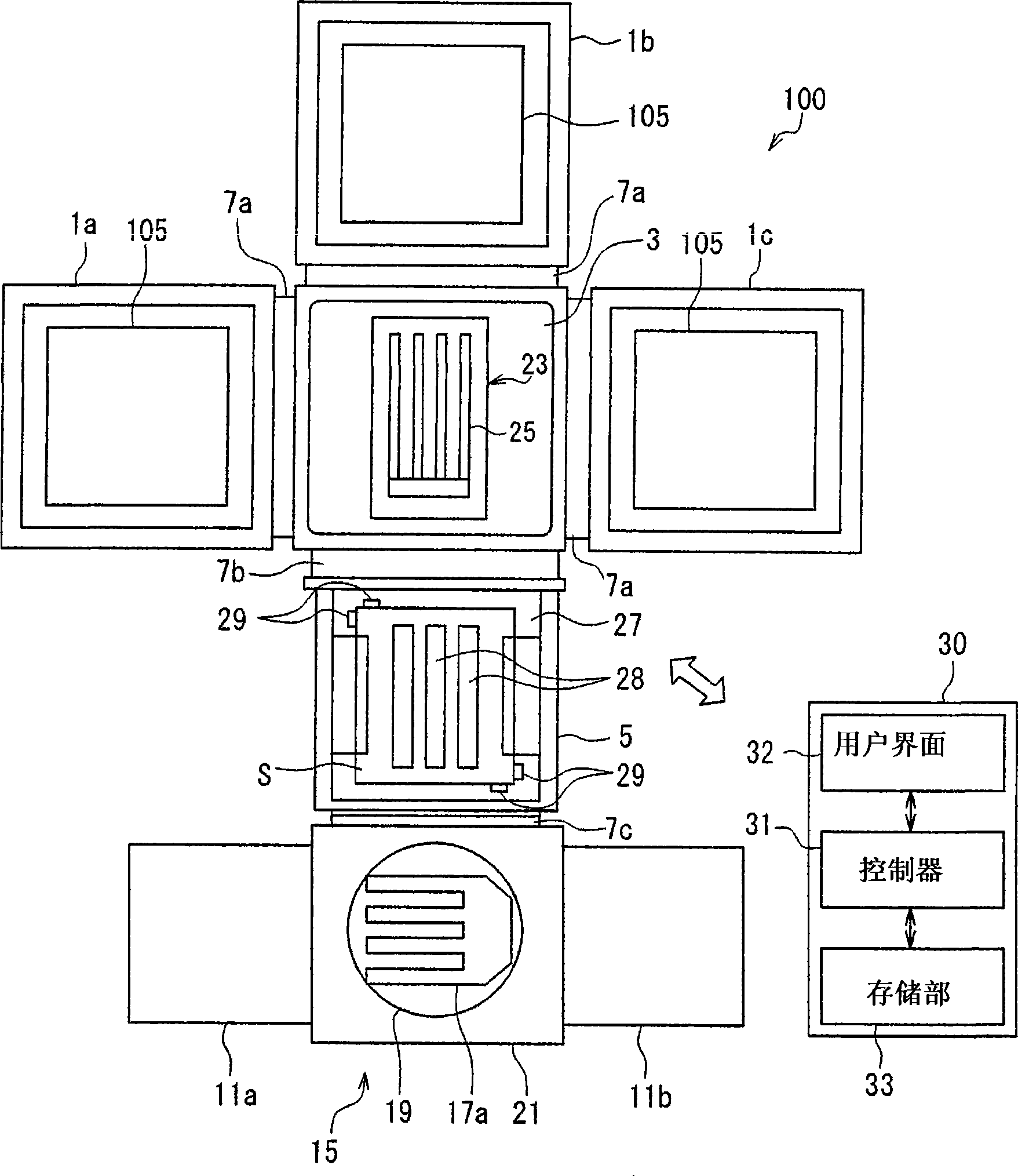
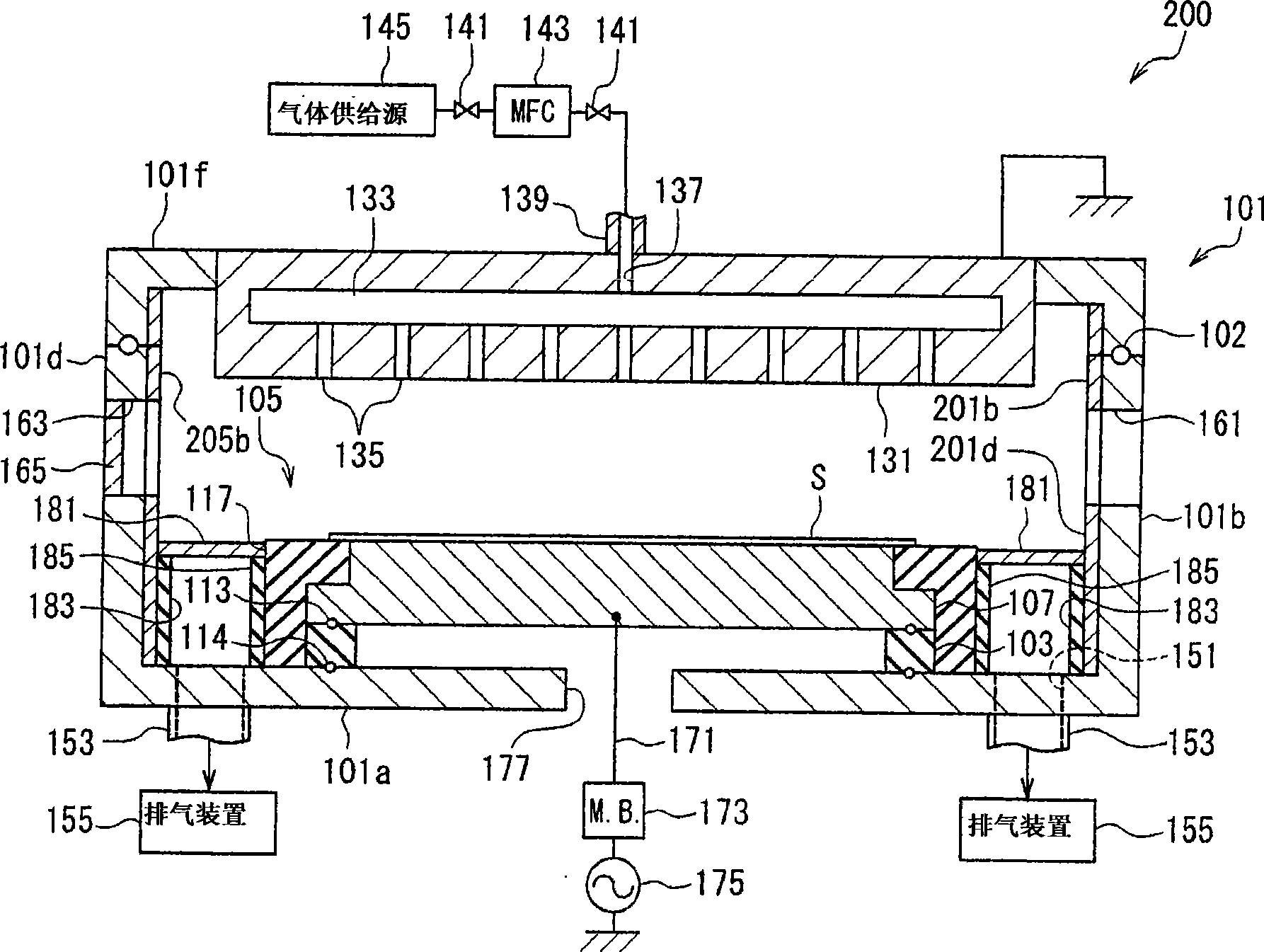
[0061] Hereinafter, embodiments of the present invention will be described in detail with reference to the drawings. Here, a substrate processing system including the processing container according to the first embodiment of the present invention will be described as an example. figure 1 is a perspective view briefly showing a vacuum processing system 100 as a substrate processing system; figure 2 This is a plan view schematically showing the interior of each chamber with a lid (not shown) in an open state. The vacuum processing system 100 has a multi-chamber structure including processing chambers 1a, 1b, and 1c. The vacuum processing system 100 is configured, for example, as a processing system for performing plasma processing on a glass substrate (hereinafter, simply referred to as "substrate") S for FPD. Among them, examples of the FPD include a liquid crystal display (LCD), an electroluminescence (EL) display, a plasma display panel (PDP), and the like.
[0062] In th...
no. 2 approach
[0114] Next, refer to Figure 6 ~ Figure 11 , the second embodiment of the present invention will be described. Image 6 It is a schematic diagram showing the inside of the processing container according to the second embodiment of the present invention. Here, the inner wall surfaces of the side wall 101 b having the substrate transfer opening 161 and the side wall 101 c having the window opening 163 of the processing container 101 are shown.
[0115] The inner surface of the side wall 101b having the substrate transfer opening 161 is covered with a plate-shaped main pad 211 as a first protection member, thereby being protected from plasma and corrosive gas. The main pad 211 has an opening corresponding to the size of the substrate transfer opening 161 .
[0116] Around the corners 161a at both ends of the substrate transfer opening 161, auxiliary pads 301a and 301b as second protective members, which are formed in smaller pieces than the main pad 211, are stacked on the mai...
PUM
 Abstract
Description
Claims
Application Information
 - R&D
- Intellectual Property
- Life Sciences
- Materials
- Tech Scout
- Unparalleled Data Quality
- Higher Quality Content
- 60% Fewer Hallucinations
Browse by: Latest US Patents, China's latest patents, Technical Efficacy Thesaurus, Application Domain, Technology Topic, Popular Technical Reports.
© 2025 PatSnap. All rights reserved.Legal|Privacy policy|Modern Slavery Act Transparency Statement|Sitemap|About US| Contact US: help@patsnap.com


