Pixel structure, display panel and method for manufacturing optoelectronic device

A manufacturing method and technology of pixel structure, applied in the field of display panel and optoelectronic device manufacturing, pixel structure, can solve the problems of high production cost, complicated steps, inability to effectively increase production capacity, etc., to increase production capacity, shorten process time, capacitance Value boost effect

Active Publication Date: 2009-04-15
AU OPTRONICS CORP
View PDF0 Cites 19 Cited by
  • Summary
  • Abstract
  • Description
  • Claims
  • Application Information

AI Technical Summary

Problems solved by technology

[0004] In the known technology, at least seven photomask processes are required to manufacture the color filter layer on the thin film transistor array, and the color filter pattern needs to be manufactured through three photomask processes, so the steps are complicated higher production costs
In addition, the above-mentioned pixel structure requiring at least seven photomask processes needs to use multiple photomasks with different patterns. Since the cost of photomasks is very expensive, the manufacturing cost of the pixel structure will not be reduced. And due to the large number of photomasks, the production capacity cannot be effectively improved

Method used


Image

  • Pixel structure, display panel and method for manufacturing optoelectronic device
  • Pixel structure, display panel and method for manufacturing optoelectronic device
  • Pixel structure, display panel and method for manufacturing optoelectronic device

Examples


Embodiment Construction

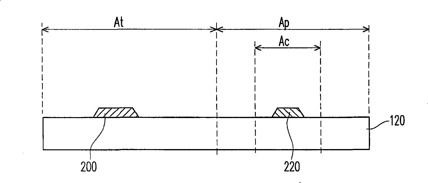
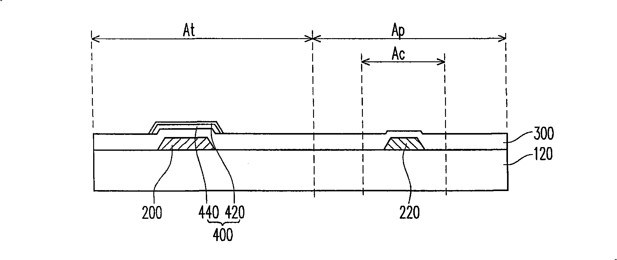
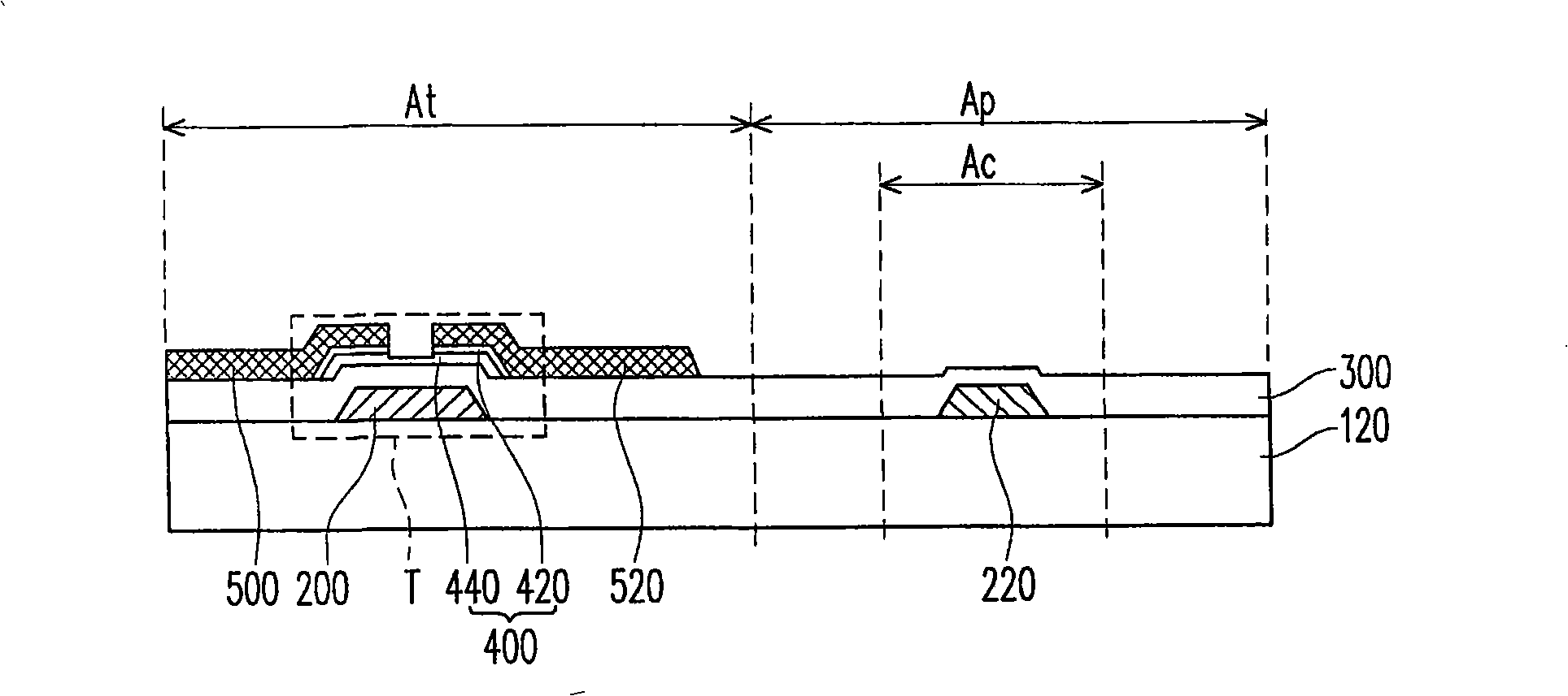
[0064] Figure 1A to Figure 1J is a schematic cross-sectional view of a method for manufacturing a pixel structure according to an embodiment of the present invention, wherein Figure 1A ~ Figure 1J A pixel structure is used as a representative for illustration. First, please refer to Figure 1A , the substrate 120 is provided, and the substrate 120 has a transistor region At, a capacitor region Ac and a pixel region Ap. In the present invention, one of the transistor region At, the capacitor region Ac and the pixel region Ap is illustrated as an example, but not limited thereto. In other embodiments, at least one of the transistor region At, the capacitor region Ac, and the pixel region Ap can be at least one of the above-mentioned ones according to design requirements, such as: different visible regions, increased capacitance, different control capabilities, etc., can be at least more than one. Next, the gate 200 is formed in the transistor region At of the substrate 120 ...


PUM


Abstract

The invention provides methods for manufacturing a pixel structure, a display panel and a photoelectrical device. The method for manufacturing the pixel structure comprises the steps as follows: firstly, a baseplate is provided and is provided with a transistor area, a capacitor area and a pixel area; subsequently, a film transistor and a capacitor electrode are formed on the baseplate, wherein, the capacitor electrode is covered by a dielectric layer; then, a color filter layer is formed on the film transistor and the capacitor electrode, and a protection layer is formed on the color filter layer; patterned photoresist layers with different thicknesses are formed on the protection layer, and partial protection layer and partial patterned photoresist layers are removed sequentially to expose partial source / drain electrode of the film transistor and partial protection layer; then, the protection layer is covered by a conductive layer in a conformal way, and partial patterned photoresist layer is removed to define a pixel electrode. The invention can reduce the manufacturing cost, shorten technical time and increase the productivity, and the capacitance value of the capacitance stored in the pixel structure is improved effectively.

Description

technical field [0001] The present invention relates to a manufacturing method of a pixel structure, a display panel and an optoelectronic device, and in particular to a manufacturing method of a pixel structure capable of reducing the number of photomasks, and a manufacturing method of a display panel and an optoelectronic device having the pixel structure. Background technique [0002] Liquid crystal displays have the advantages of high image quality, small size, light weight, low voltage drive, low power consumption, and wide application range. Therefore, they have replaced cathode ray tubes (Cathode Ray Tube, CRT) and become the mainstream of the new generation of displays. At present, the market is oriented toward high contrast ratio, no gray scale inversion, high brightness, high color saturation, fast response ( response) and wide viewing angle (viewing angle) and other directions. Currently common wide viewing angle technologies include: twisted nematic liquid cryst...

Claims


Application Information

Patent Timeline
IPC IPC(8): H01L21/84G02F1/1362
Inventor 曾贤楷廖金阅陈建宏
Owner AU OPTRONICS CORP
Why Eureka
Try Eureka