Semi-conductor device and time clock recovery method and device

A technology of clock recovery and optical devices, which is applied in the field of optical networks, can solve problems such as low integration and limited filter fineness parameters, and achieve the effects of overcoming harsh requirements, simple structure, and easy implementation

Active Publication Date: 2009-04-01
HUAWEI TECH CO LTD +1
View PDF0 Cites 2 Cited by
  • Summary
  • Abstract
  • Description
  • Claims
  • Application Information

AI Technical Summary

Problems solved by technology

Therefore, it can overcome the problem that the existing clock recovery scheme is not highly integrated and is limited by the fineness parameters of the filter

Method used


Image

  • Semi-conductor device and time clock recovery method and device
  • Semi-conductor device and time clock recovery method and device
  • Semi-conductor device and time clock recovery method and device

Examples


Embodiment Construction

[0030] The invention provides a semiconductor optical device and a clock recovery method and device.

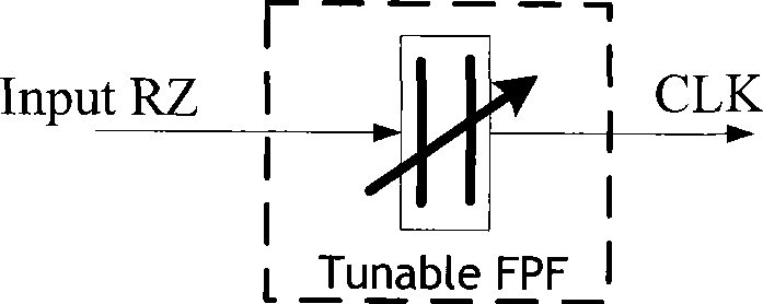
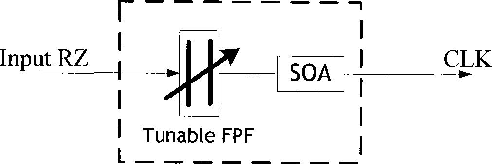
[0031] The present invention will be described in detail below in conjunction with the accompanying drawings. The structural diagram of the embodiment of the clock recovery device of the present invention is as follows Figure 4 As shown, it includes: a signal input unit, a semiconductor optical device and a signal output unit.

[0032] The signal input unit receives the input optical signal and transmits the optical signal to the semiconductor optical device through the input optical fiber.

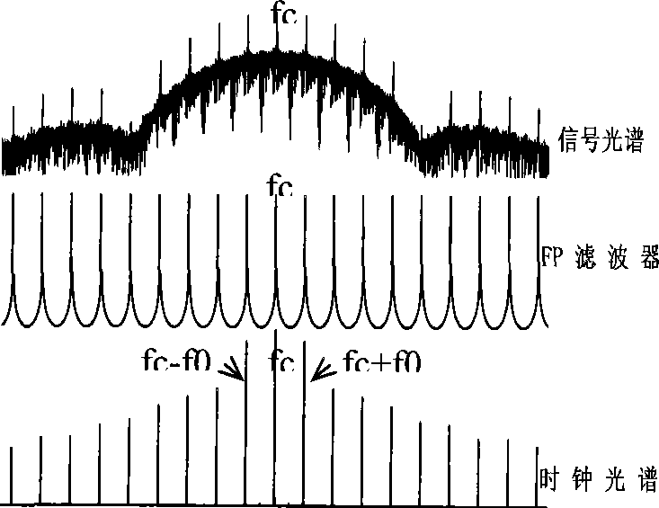
[0033] After comb filtering the optical signal, the semiconductor optical device recovers the clock signal from the optical signal, and transmits the clock signal to the output optical fiber.

[0034] The signal output unit outputs the clock signal through the output optical fiber.

[0035] By controlling the end face reflectivity of the above-mentioned semiconductor optical device wi...


PUM


Abstract

The invention provides a semiconductor optical device, a clock recovery method and a device thereof. Two end faces of an epitaxial wafer of the semiconductor optical device are provided with an end face antireflection coating which is used for comb filtering processing of a received optical signal; reflectivity of the end face is set according to amplitude jitter rate of a clock signal output from the semiconductor optical device, thus quality of the clock signal output from the semiconductor optical device is controlled within a set range. All-optical clock recovery of different rates can be realized by properly selecting the end face reflectivity of the semiconductor optical device, thus causing the quality of the recovered clock signal to be within the set range.

Description

technical field [0001] The invention relates to the field of optical networks, in particular to a semiconductor optical device and a clock recovery method and device. Background technique [0002] In a high-speed and large-capacity optical network, there are some factors that will obviously affect the quality of the optical signal, such as code pattern, line loss, ASE (Amplified Spontaneous Emission, amplified spontaneous emission) noise of the optical amplifier, GVD (Group Velocity Dispersion , Group Velocity Dispersion), PMD (Polarisation Mode Dispersion, Polarization Mode Dispersion) and nonlinear effects will affect the shape of the signal, the optical signal-to-noise ratio and the extinction ratio, make the pulse broaden and generate timing jitter, resulting in signal quality degradation. [0003] 3R (Regenration, Reshaping, Retiming, regeneration, reshaping and retiming) regeneration is an effective method to solve the above problems. All-optical clock recovery in 3R ...

Claims


Application Information

Patent Timeline
IPC IPC(8): H04B10/17H04B10/02
CPCH01S5/0287H01S5/1039H01S5/168H01S5/028H01S5/0622H01S5/5045
Inventor 张新亮余宇傅炜
Owner HUAWEI TECH CO LTD
Why Eureka
Try Eureka