Wafer

A chip and substrate technology, applied in the direction of electrical components, electrical solid devices, circuits, etc., can solve problems such as difficult to print identification codes, misidentification of reading identification codes, and problems with productivity, so as to increase production quantity and expand devices area, the effect of accurate identification

Active Publication Date: 2009-03-11
DISCO CORP
View PDF3 Cites 2 Cited by
  • Summary
  • Abstract
  • Description
  • Claims
  • Application Information

AI Technical Summary

Problems solved by technology

[0009] However, when the identification code is printed on the back of the wafer, there is a problem that if the back of the wafer is ground to form the wafer to a predetermined thickness, the printed identification code will disappear.
[0010] In addition, if the identification code is printed on the surface of the wafer, the area where the device can be formed is limited. At the same time, when the back surface of the wafer is ground to form the wafer to a predetermined thickness, if the identification code is pasted on the surface of the wafer If the protective belt is worn by BG, the identification code cannot be recognized
[0011] In addition, if the identification code is printed on the outer peripheral surface of the wafer, since the outer peripheral surface of the wafer is formed with a chamfer formed by a circular arc surface, it is difficult to print the identification code, and there may be errors in reading the identification code. identify
[0012] In addition, if the identification code is printed on the positioning plane showing the orientation of the crystal formed on the outer periphery of the wafer, although the above-mentioned problem is solved, the area where the device is formed on the wafer with the positioning plane is reduced, so there is a disadvantage in terms of productivity. question

Method used


Image

  • Wafer
  • Wafer
  • Wafer

Examples


Embodiment Construction

[0026] Hereinafter, preferred embodiments of a wafer constructed according to the present invention will be described in detail with reference to the accompanying drawings.

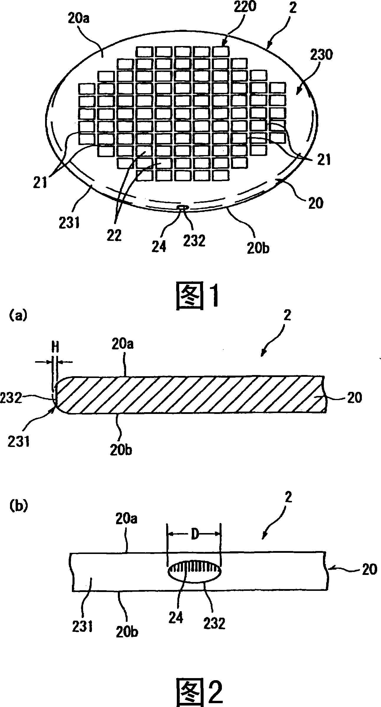
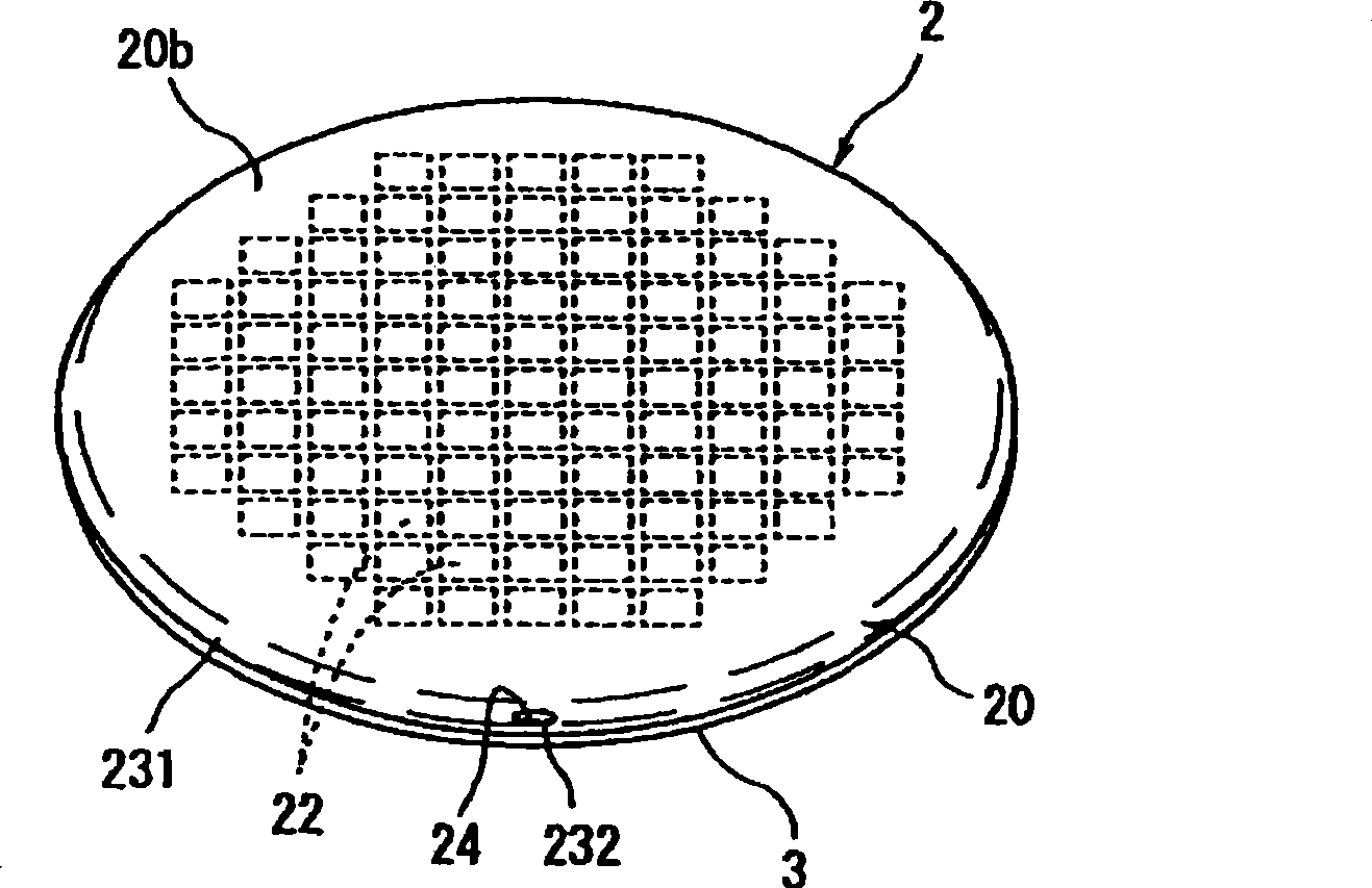
[0027] FIG. 1 shows a perspective view of a semiconductor wafer as a wafer constructed according to the present invention. In the semiconductor wafer 2 shown in FIG. 1 , on the surface 20a of a wafer substrate 20 made of, for example, silicon with a thickness of 700 μm, a plurality of blank channels 21 are arranged in a grid pattern, and at the same time, when divided by the multiple blank channels 21 Devices 22 such as ICs and LSIs are formed in a plurality of regions. The wafer substrate 20 thus formed has a device region 220 where a plurality of devices 22 are formed and a peripheral remaining region 230 surrounding the device region 220 . In addition, in order to prevent cracks and breakage due to inadvertently received impacts, as shown in FIG. 20b forms a chamfer 231 whose cross-sectional shape is...


PUM


Abstract

A wafer having a device region, where a plurality of devices is formed, and an outer peripheral surplus region, which surrounds the device region, on the face of a circular wafer substrate is disclosed. A chamfered portion whose cross-sectional shape defines an arc-shaped surface in a range from the face to the back of the wafer substrate is formed in an outer peripheral end portion of the outer peripheral surplus region of the wafer substrate. A flat surface orthogonal to the face and the back is formed in the chamfered portion as a mark showing the crystal orientation of the wafer substrate. An identification code for specifying the wafer substrate is printed on the flat surface.

Description

technical field [0001] The present invention relates to wafers such as semiconductor wafers in which devices such as ICs and LSIs are formed on the surface of a wafer substrate. Background technique [0002] In the manufacturing process of a semiconductor device, on the surface of a substantially circular plate-shaped wafer substrate, a plurality of regions are divided by dividing predetermined lines called blank channels (streets) arranged in a network, and through the divided regions IC, LSI and other devices are formed to form a semiconductor wafer. The semiconductor wafer formed in this way is cut along the blank channel to divide the region where the device has been formed, and each device is manufactured. In addition, optical device wafers such as gallium nitride-based compound semiconductors are laminated on the surface of a sapphire substrate, and are also divided into individual optical devices such as light-emitting diodes and laser diodes by cutting along blank c...

Claims


Application Information

Patent Timeline
Patent Type & Authority Applications(China)
IPC IPC(8): H01L23/544
CPCH01L21/67092H01L21/304H01L2223/54413H01L2223/54453H01L2221/6834H01L2223/54493H01L23/544H01L2924/0002H01L2223/54433H01L2924/00H01L21/302
Inventor 关家一马
Owner DISCO CORP
Why Eureka
Try Eureka