Method for manufacturing detection chip for measuring and checking numbers of particles and defects on chip

A defect count and chip detection technology, which is applied in the preparation of test samples, measurement devices, semiconductor/solid-state device testing/measurement, etc.

Inactive Publication Date: 2009-02-11
MACRONIX INT CO LTD
View PDF0 Cites 2 Cited by
  • Summary
  • Abstract
  • Description
  • Claims
  • Application Information

AI Technical Summary

Problems solved by technology

[0007] The main problem to be solved by the present invention is to provide a method for manufacturing a detection chip capable of measuring the number of particles and defects on the detection chip, which can quickly and effectively detect the metal pollution and particle content in the process device, so as to solve the problem of existing detection problems. The problem with the method

Method used


Image

  • Method for manufacturing detection chip for measuring and checking numbers of particles and defects on chip
  • Method for manufacturing detection chip for measuring and checking numbers of particles and defects on chip
  • Method for manufacturing detection chip for measuring and checking numbers of particles and defects on chip

Examples


Embodiment Construction

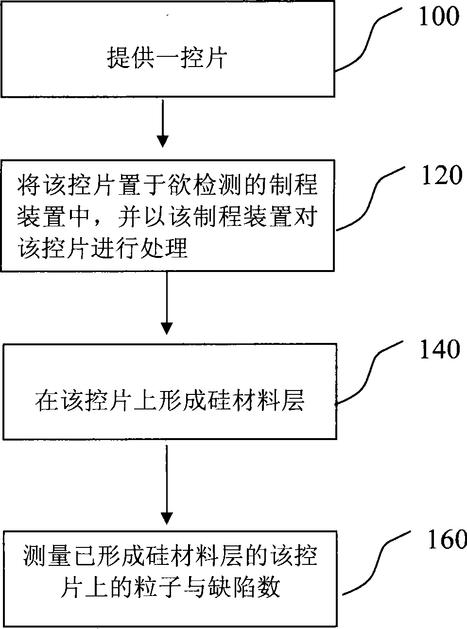
[0030] Please refer to figure 1 , figure 1 It is a flow chart of the steps of the method for detecting metal pollution and microparticles in a process device by using a control chip.

[0031] Step 100: Provide a control sheet such as a blank chip or a control sheet without graphics.

[0032] Step 120: Place the control piece in a process device to be tested, such as one of the machine equipment used in the processes of thin film deposition, dry etching, ion implantation and lithography, and compare the control with the process device The wafer is processed by one of the processes of thin film deposition, dry etching, ion implantation and lithography.

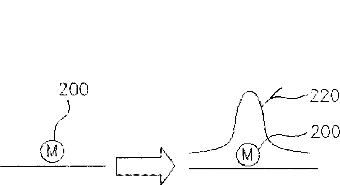
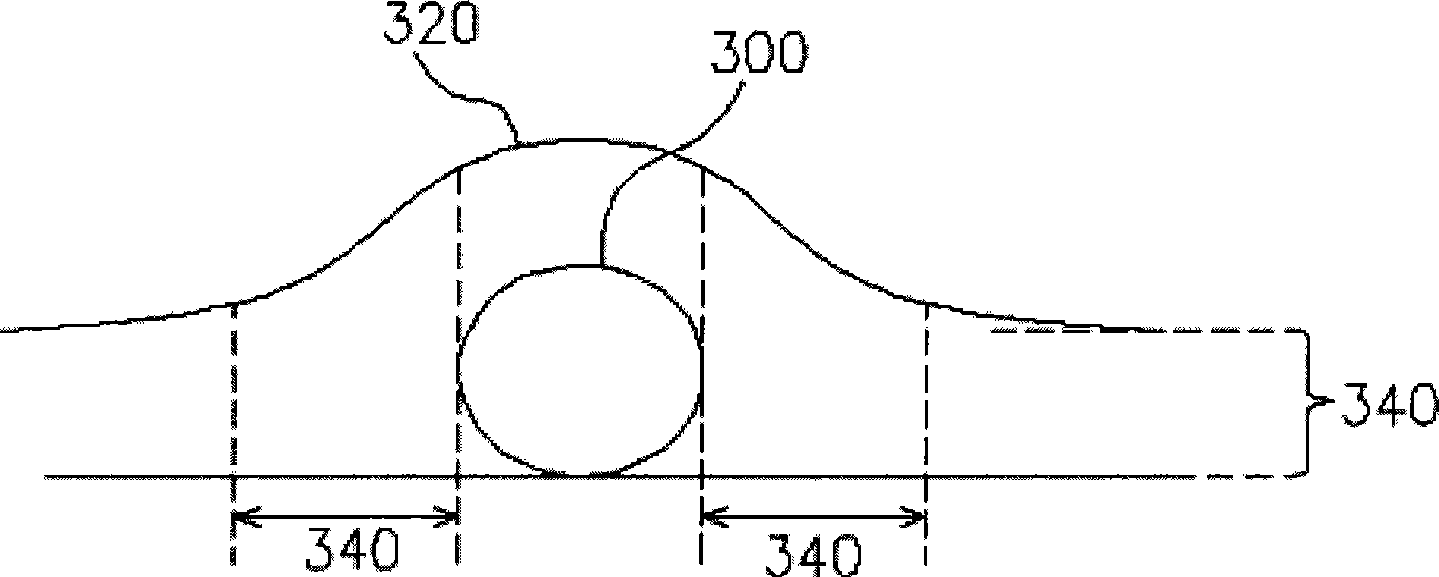
[0033] Step 140: Form a silicon material layer on the control chip (for example, the silicon material layer is polysilicon, amorphous silicon and epitaxial silicon), and the formation method of the silicon material layer can be, for example, chemical vapor deposition. When the silicon material layer is formed on the control ch...


PUM

PropertyMeasurementUnit
thicknessaaaaaaaaaa

Abstract

The invention relates to method for manufacturing a detection chip for measuring and inspecting the particles and the number of defects on a chip. The method comprises the steps of providing a blank chip; placing the blank chip in a manufacture procedure device to be detected; using the manufacture procedure device to process the blank chip; and forming a silicon material layer on the blank chip. The blank chip with silicon material layer can directly measure the particles and the number of defects, that is, the metal pollution and the micro-particle pollution degree in the manufacture procedure device can be obtained.

Description

[0001] This application is a divisional application with an application date of April 22, 2003, an application number of 03122159.9, and an invention title of "Metal Contamination and Microparticle Detection Method in Process Equipment". technical field [0002] The invention relates to a method for detecting metal pollution and microparticles, in particular to a method for manufacturing a semiconductor detection chip capable of measuring the number of particles and defects on the inspection chip. Background technique [0003] The so-called integrated circuit is an electronic product that reduces and manufactures various components and circuits required for a specific circuit in an area of ​​only 2 cm or less. Because integrated circuits are mostly composed of tens of thousands of solid-state electronic components whose size can only be viewed with a microscope, they can also be called microelectronic components. [0004] The current technology development trend of semicondu...

Claims


Application Information

Patent Timeline
Patent Type & Authority Applications(China)
IPC IPC(8): G01N1/28G01N23/223H01L21/66
Inventor 俞文光黄良田
Owner MACRONIX INT CO LTD
Why Eureka
Try Eureka