Device for adhering various cells on same substrate orderly and adhering method
A substrate and cell technology, which is applied in the field of devices and adhesions that adhere multiple cells to the same substrate in an orderly array, and can solve problems such as difficult construction of cell arrays, inability to interact, complex chemical synthesis, etc.
- Summary
- Abstract
- Description
- Claims
- Application Information
AI Technical Summary
Problems solved by technology
Method used
Image
Examples
Embodiment 1
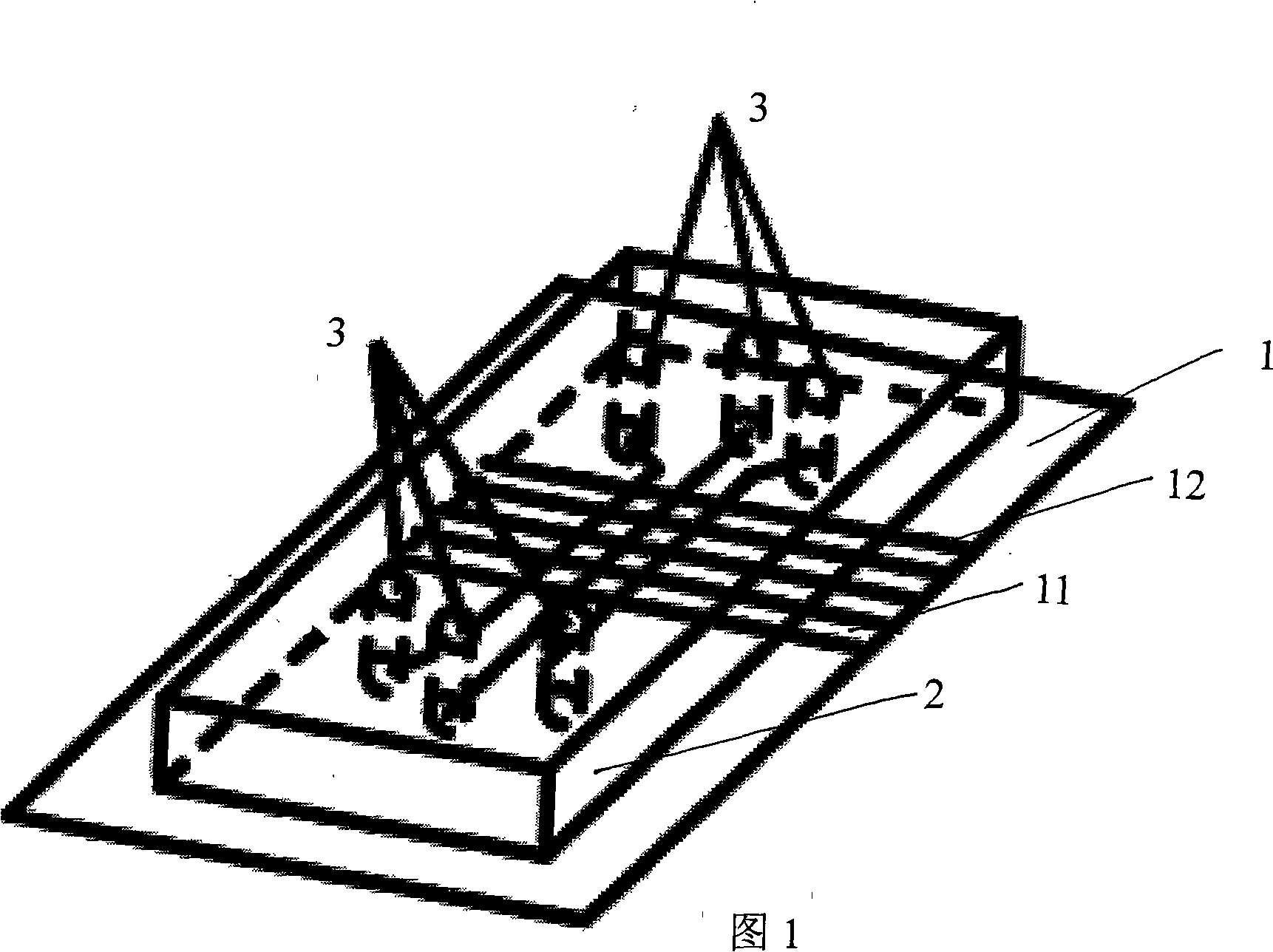
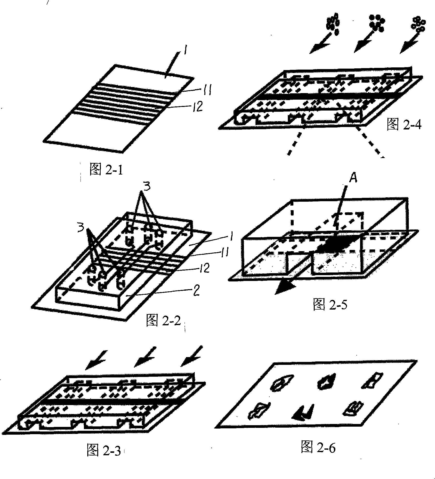
[0040] Please refer to Figure 2-1, Figure 2-2, Figure 2-3, Figure 2-4, Figure 2-5 and Figure 2-6:
[0041] 1) Evaporating a 2-10 nm thick titanium adhesion layer on the upper surface of a clean glass substrate 1, and then evaporating a 20-50 nm thick gold layer thereon;
[0042] 2) Using photolithography technology, prepare an array structure with 50 parallel convex strips with a width of 100 μm (20-300 μm is acceptable), a length of 2 cm, and an interval of 200 μm on a silicon wafer;
[0043] 3) Flip the silicon wafer having an array structure of 50 parallel convex strips obtained in step 2) with polydimethylsiloxane, and obtain a silicon wafer corresponding to the array structure of the parallel convex strips. The first polydimethylsiloxane stamp with an array structure of 49 parallel convex strips;
[0044] Put the resulting stamp into 10 mM methyl terminated thiol (molecular formula: HS(CH 2 ) 11 CH 3 ) in the ethanol solution; then take it out, dry it with nitrogen or...
Embodiment 2
[0053] 1) First evaporate a 5nm (2-10nm) thick titanium adhesion layer on the upper surface of a clean glass slide (thickness 0.15mm), and then evaporate a 40nm (20-50nm) thick titanium adhesion layer on it ) a thick gold layer to make a test substrate 1;
[0054] 2) Using photolithography technology, prepare an array structure with 100 parallel convex strips with a width of 100 μm (20-300 μm is acceptable), a length of 2 cm, and an interval of 100 μm (20-300 μm is acceptable) on a silicon wafer ;
[0055] 3) Flip the silicon wafer with an array structure of 100 parallel convex strips obtained in step 2) with polydimethylsiloxane, to obtain a film corresponding to the array structure of the parallel convex strips. The first polydimethylsiloxane stamp with an array structure of 99 parallel convex strips;
[0056] Put the resulting stamp into 10 mM methyl terminated thiol (molecular formula: HS(CH 2 ) 15 CH 3 or HS(CH2) 17 CH 3 ) in the ethanol solution; then take it out,...
PUM
 Abstract
Description
Claims
Application Information
 - R&D
- Intellectual Property
- Life Sciences
- Materials
- Tech Scout
- Unparalleled Data Quality
- Higher Quality Content
- 60% Fewer Hallucinations
Browse by: Latest US Patents, China's latest patents, Technical Efficacy Thesaurus, Application Domain, Technology Topic, Popular Technical Reports.
© 2025 PatSnap. All rights reserved.Legal|Privacy policy|Modern Slavery Act Transparency Statement|Sitemap|About US| Contact US: help@patsnap.com


