Method and apparatus for forming self-aligning common source electrode in a memory structure

A self-aligned, common source technology, used in semiconductor/solid-state device manufacturing, electrical components, circuits, etc., to solve problems such as inability to maintain erase performance and reduce component size

Active Publication Date: 2008-12-24
SEMICON MFG INT (SHANGHAI) CORP
View PDF0 Cites 6 Cited by
  • Summary
  • Abstract
  • Description
  • Claims
  • Application Information

AI Technical Summary

Problems solved by technology

This makes it impossible to reduce the size of the component while maintaining the original erase performance

Method used


Image

  • Method and apparatus for forming self-aligning common source electrode in a memory structure
  • Method and apparatus for forming self-aligning common source electrode in a memory structure
  • Method and apparatus for forming self-aligning common source electrode in a memory structure

Examples


Embodiment Construction

[0026] The preferred embodiments of the present invention will be described in detail below in conjunction with the accompanying drawings, in which similar structures use the same reference numerals.

[0027] Method for forming self-aligned common source in memory structure

[0028] Refer to the following Figure 6 A method of forming a self-aligned common source according to an embodiment of the present invention is described.

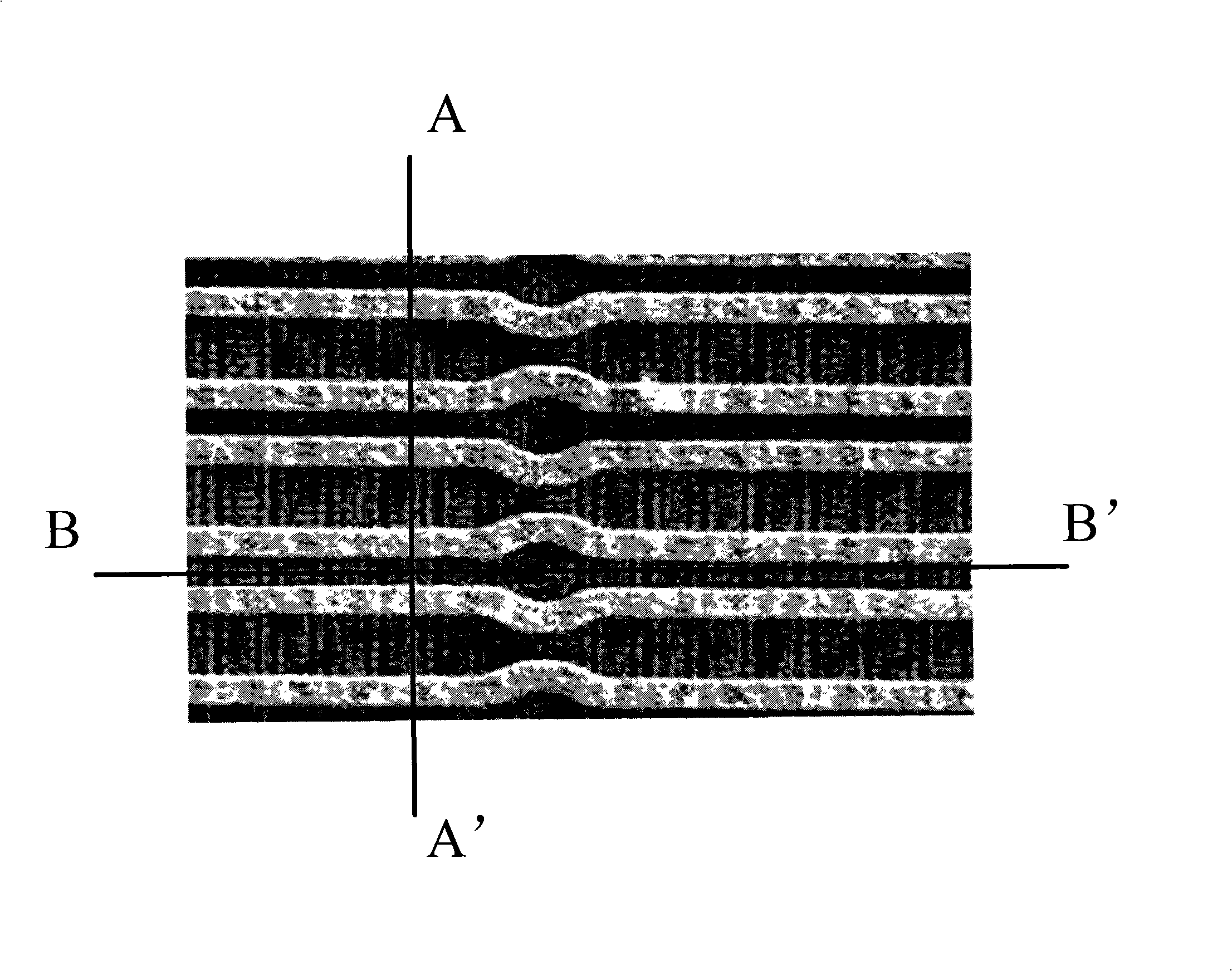
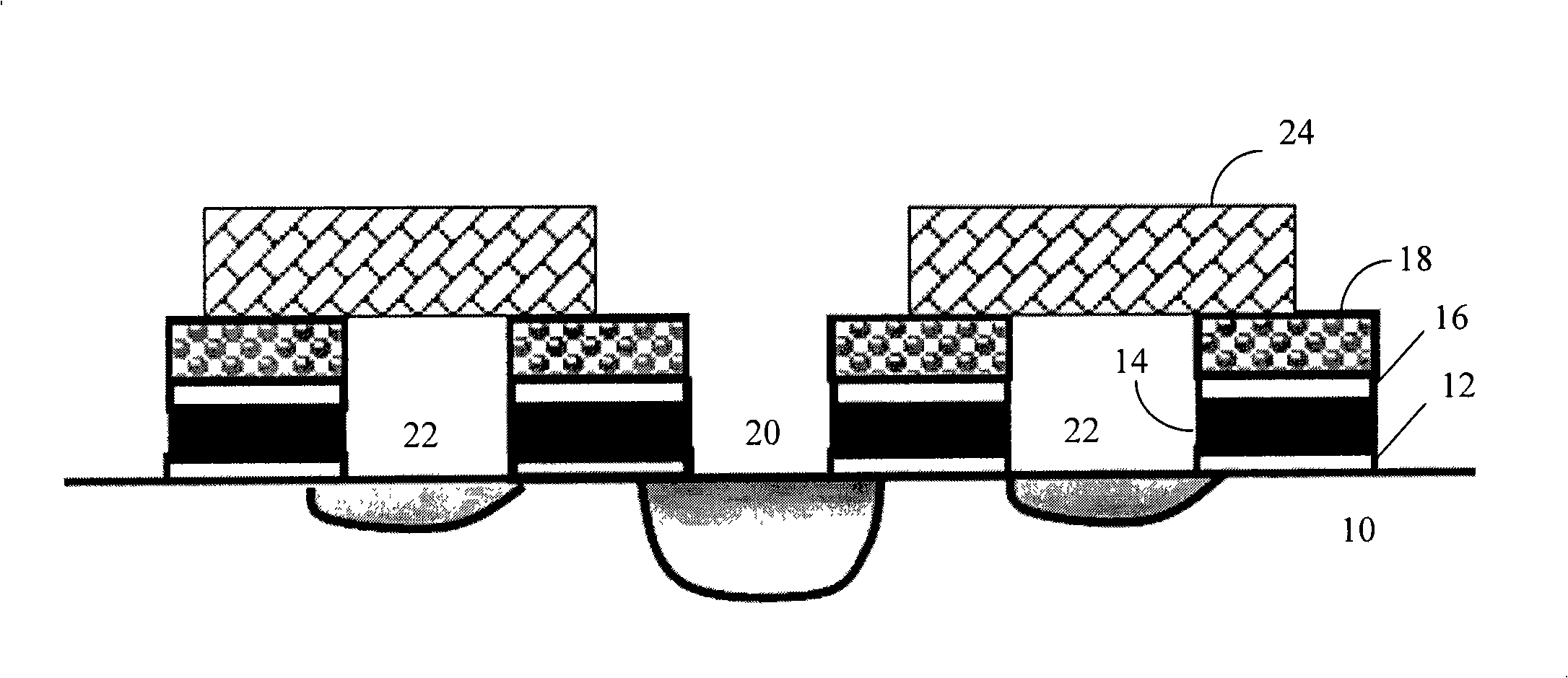
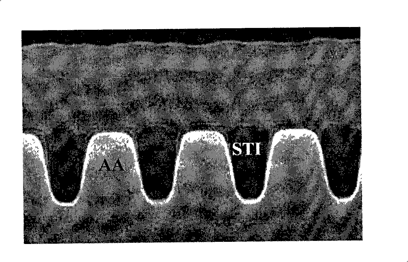
[0029] Before forming a self-aligned common source, such as image 3 As shown, alternate active areas (AA) and shallow trench isolation regions (STI) are formed on the surface of the substrate. After that, refer to figure 2 , generate an oxide layer 12 on the substrate 10, and then sequentially generate a first polycrystalline layer 14, a dielectric layer 16, and a second polycrystalline layer 18 on it to form a multilayer structure, and then pattern the multilayer structure. A source region 20 and a drain region 22 are formed on the base, and t...


PUM


Abstract

The invention provides a method for forming a self-aligned common source, which is used in a memory construction and comprises the steps as follows: a plurality of word wires are formed on a substrate, wherein, two sides of each word wire are a source area and a drain area respectively; photoetching is carried out to the source areas to form a photoresist layer, wherein, the photoresist layer covers the drain areas and parts of the word wires; the source areas that are not covered by the photoresist layer are etched so that all the source areas are communicated to form a common source area on which ion implantation is carried out by ion beams to form the self-aligned common source; the direction in which the ion beams are implanted and a normal on the surface of the substrate are separated by a slant angle. In addition, the invention also provides a device for realizing the method. By adopting the technical proposal of the invention, the lateral doping concentration under the boundary of the common source is obviously increased, thus ensuring that under the circumstance that the size of the source area is reduced continuously the resistance of the common source can always be kept at the same level as the common source of large area, and the resistance value of the common source is reduced to a range meeting the requirements.

Description

technical field [0001] The present invention generally relates to memory manufacturing processes, and more particularly to methods and devices for forming self-aligned common sources in memory structures. Background technique [0002] In a memory manufacturing process such as a flash memory, a Self-Aligned Common-Source (SAS) structure is employed. Such as figure 2 As shown, a partial cross-sectional view of a typical flash memory cell to be formed into a SAS is shown, which is based on figure 1 The cross-sectional view obtained on the A-A' plane in . Usually before forming the self-aligned common source structure, such as image 3 as shown ( image 3 so figure 1 The cross-sectional view obtained on the B-B' plane in ), before the word line is formed, through active area lithography and active area etching, alternate active areas (AA) and shallow trench isolation areas will be formed on the surface of the substrate (STI). In the subsequent process, each component is...

Claims


Application Information

Patent Timeline
IPC IPC(8): H01L21/8247H01L21/265
Inventor 吴佳特李绍彬高建玉
Owner SEMICON MFG INT (SHANGHAI) CORP
Why Eureka
Try Eureka