
Layout for reducing aberration sensitiveness, light shield manufacture and graphic method

A technology of layout method and manufacturing method, which is applied in the direction of photoplate making process, optics, and originals for photomechanical processing on the pattern surface, which can solve the problems of reducing the sensitivity of the lithography system to aberrations and achieve the best critical size Consistency, reduced aberration sensitivity, improved density distribution and uniformity effects

Inactive Publication Date: 2008-12-24
SEMICON MFG INT (SHANGHAI) CORP
View PDF1 Cites 12 Cited by
  • Summary
  • Abstract
  • Description
  • Claims
  • Application Information

AI Technical Summary

Problems solved by technology

However, for the above-mentioned technical solution, for the mask pattern whose pattern pitch is greater than CD, the auxiliary patterns located above and below the pattern can only compensate the influence of aberration to a certain extent and improve the CD consistency of the pattern, but cannot fundamentally Reduce the sensitivity of the lithography system to aberrations

Method used


Image

  • Layout for reducing aberration sensitiveness, light shield manufacture and graphic method
  • Layout for reducing aberration sensitiveness, light shield manufacture and graphic method
  • Layout for reducing aberration sensitiveness, light shield manufacture and graphic method

Examples


no. 1 example

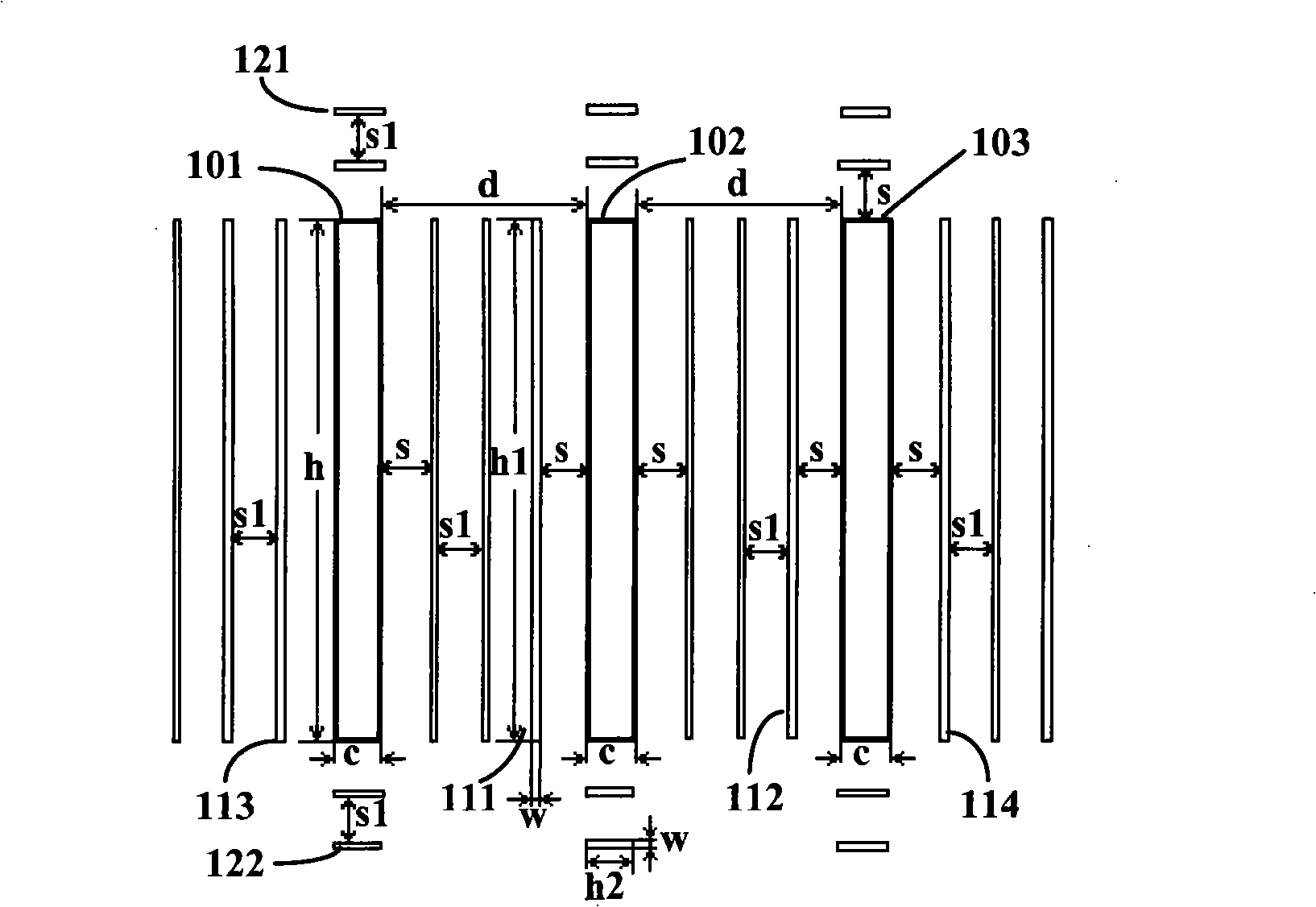
[0025] Please refer to figure 1 , figure 1 It is a schematic diagram of adding layout auxiliary graphics to one-dimensional layout patterns in the layout method for reducing aberration sensitivity described in the present invention. As shown in the figure, the layout patterns 101, 102, 103 parallel to each other form a one-dimensional layout pattern, and the width c of the layout patterns 101, 102, 103 is 1CD. According to the distance between the layout graphics 101, 102, 103, the layout graphics can form a one-dimensional dense pattern, a one-dimensional semi-dense pattern, or a one-dimensional isolated pattern. The dense pattern means that the distance between the layout graphics is equal to 1CD, semi-dense A pattern means that the distance between the layout graphics is greater than 1CD and less than or equal to 3CD, and an isolated pattern means that the distance between the layout graphics is greater than 3CD. In this embodiment, the spacing d of the layout patterns 10...

no. 2 example

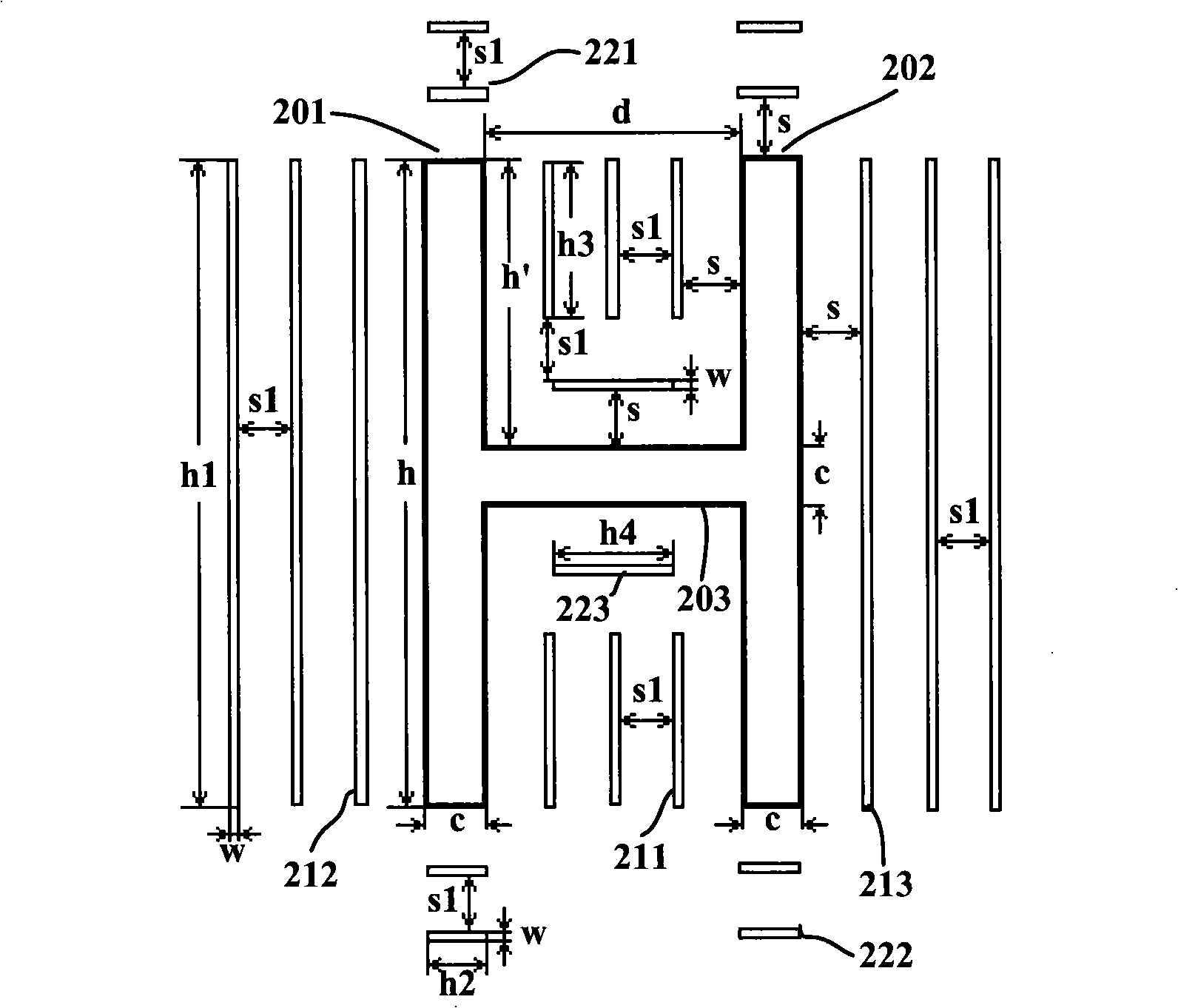
[0030] Please refer to figure 2 , figure 2 It is a schematic diagram of adding layout auxiliary graphics to two-dimensional layout patterns in the layout method for reducing aberration sensitivity described in the present invention, wherein it is the same as figure 1 The same symbols represent the same or similar meanings. As shown in the figure, the layout pattern 203 is perpendicular to and connects the layout patterns 201 and 202, that is, constitutes a two-dimensional layout pattern. The width c of the layout patterns 201, 202 and 203 is 1CD. According to the distance between the layout graphics 201 and 202, the layout graphics can form a two-dimensional dense pattern, a two-dimensional semi-dense pattern or a two-dimensional isolated pattern. The dense pattern means that the distance between the layout graphics is equal to 1CD, and the semi-dense pattern means The distance between the layout graphics is greater than 1CD and less than or equal to 3CD, and the isolated ...


PUM


Abstract

The invention relates to a layout method for reducing aberration sensitivity, which is characterized in that at least one layout auxiliary graph is added around a layout graph, the layout auxiliary graphs are not intersected mutually, the layout auxiliary graphs and the layout graph are not intersected mutually, the distance between the neighboring layout auxiliary graphs is longer than or equal to one time of the critical dimension of the layout graph, and shorter than or equal to three times of the critical dimension of the layout graph. The invention also discloses a manufacturing method of a photomask for reducing the aberration sensitivity, and an imaging method. By applying the methods provided by the invention, the aberration sensitivity of a photoetching system can be reduced, which causes the graphs formed on the photoetching cellophane of a semiconductor substrate to obtain better critical dimension uniformity.

Description

technical field [0001] The invention relates to the technical field of semiconductor manufacturing, in particular to a layout, photomask manufacturing and patterning method capable of reducing the aberration sensitivity of a photolithography system. Background technique [0002] With the rapid development of semiconductor manufacturing technology, in order to achieve faster computing speed, larger data storage capacity and more functions of semiconductor devices, semiconductor chips are developing in the direction of higher integration; and the integration of semiconductor chips is getting higher and higher. The higher the critical dimension (CD, Critical Dimension) of the semiconductor device is, the smaller it is. [0003] In order to realize a tiny CD, it is necessary to transfer the designed finer layout pattern to the photomask, and then use lithography (lithography) technology to focus the pattern on the photomask on the photoresist film of the semiconductor substrate,...

Claims


Application Information

Patent Timeline
Patent Type & Authority Applications(China)
IPC IPC(8): G03F1/00G06F17/50G03F1/68
Inventor 张飞
Owner SEMICON MFG INT (SHANGHAI) CORP
Learn More