Micro-cavity optical amplifier structure of 980 nanometer semiconductor with high gain and low noise

A 980nm, optical amplifier technology, applied in semiconductor lasers, the structure of optical resonators, lasers, etc., can solve the problems of large number of longitudinal modes, suppression of signal gain, and small interval of longitudinal modes, and achieve the effect of low noise and high gain

Inactive Publication Date: 2008-12-17
INST OF SEMICONDUCTORS - CHINESE ACAD OF SCI
View PDF0 Cites 3 Cited by
  • Summary
  • Abstract
  • Description
  • Claims
  • Application Information

AI Technical Summary

Problems solved by technology

Moreover, if the gain is increased by lengthening the cavity length of the traveling wave optical amplifier, the longitudinal mode spacing will be too small, so that the number of longitudinal modes participating in the mode competition will be large.
This largely limits the carrier concentration in the active region, suppressing the signal gain
For quantum wells and quantum dot vertical cavity surface optical amplifiers, the gain is not large because the active region is very thin

Method used


Image

  • Micro-cavity optical amplifier structure of 980 nanometer semiconductor with high gain and low noise
  • Micro-cavity optical amplifier structure of 980 nanometer semiconductor with high gain and low noise

Examples


Embodiment Construction

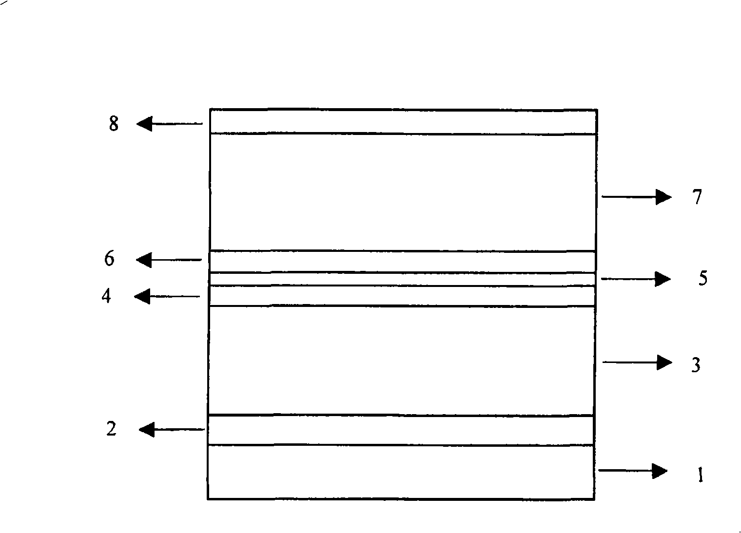
[0028] Combine below figure 1 and figure 2 Describe in detail the structure and working principle of a high-gain, low-noise 980nm semiconductor microcavity optical amplifier according to a specific embodiment of the present invention.

[0029] see figure 1 , a high-gain, low-noise 980nm semiconductor microcavity optical amplifier structure of the present invention, is characterized in that, comprises:

[0030] A substrate 1, the substrate 1 is used to make different epitaxial material layers required for growing optical amplifiers, and the substrate 1 is N-gallium arsenide material;

[0031] A buffer layer 2, the buffer layer 2 is fabricated on the substrate 1, and the buffer layer 2 is N-gallium arsenide material;

[0032] A lower Bragg reflector 3, the lower Bragg reflector 3 is made on the buffer layer 2, and the lower Bragg reflector 3 is made up of 19 cycles, N-gallium arsenide and N-aluminum arsenide layers; each cycle Both gallium arsenide and aluminum arsenide lay...


PUM


Abstract

The invention relates to a structure for a 980nm semiconductor micro-cavity optical amplifier with high gain and low noise, which is characterized in that the structure comprises a substrate, a buffer layer, a lower Bragg reflector, a lower barrier layer, a quantum well layer, an upper barrier layer, an upper Bragg reflector and an electrode contact layer, wherein the substrate is used for performing epitaxial growth of each layer of materials of the optical amplifier on the substrate; the buffer layer is made on the substrate; the lower Bragg reflector is made on the buffer layer; the lower barrier layer is made on the lower Bragg reflector; the quantum well layer is made on the lower barrier layer; the upper barrier layer is made on the quantum well layer; the upper Bragg reflector is made on the upper barrier layer; the electrode contact layer is made on the upper Bragg reflector, so as to form the micro-cavity optical amplifier. The micro-cavity optical amplifier is optically etched into a strip-shaped table surface; furthermore, two end surfaces of the table surface are etched into inclined surfaces with inclined angles of 45 degrees and coated with an anti-reflection film.

Description

technical field [0001] The invention belongs to the field of semiconductor optical amplifiers, in particular to a high-gain, low-noise 980nm semiconductor microcavity optical amplifier structure. Background technique [0002] Semiconductor optical amplifiers are important components in all-optical network transmission systems and optical fiber interconnection networks, and have a very wide range of applications and market demands in communications, military, aerospace, and private data networks. Compared with the currently dominant fiber amplifier, it has the advantages of small size, low power consumption, low cost, and easy integration with other optoelectronic devices. In the optical network, it will be widely used in relay amplification, wavelength conversion, optical switch, uplink and downlink routing, etc. Semiconductor optical amplifiers, including traveling wave optical amplifiers and vertical cavity surface optical amplifiers, have made great progress. As the req...

Claims


Application Information

Patent Timeline
Patent Type & Authority Applications(China)
IPC IPC(8): H01S5/00H01S5/10H01S5/125H01S5/343
Inventor 张泉郑厚植
Owner INST OF SEMICONDUCTORS - CHINESE ACAD OF SCI
Why Eureka
Try Eureka