


Quick Research
Generate reliable direction feasibility study reports for your R&D in just a few steps.

Technical Q&A
Discover and master advanced knowledge NOW. Basics, ideas, possibilities, all at once.

Find Solutions
As an expert in R&D theories, this can generate solutions to your technical problems instantly.

Evaluate Feasibility
Analyze your overall solution with one click, know your potential R&D risks in advance.

Monitor Landscape
Get weekly tech updates, stay abreast of the latest tech innovations and key insights.
Display device and electronic apparatus including display device
A display device and circuit technology, applied in static indicators, nonlinear optics, instruments, etc., can solve problems such as the influence of light sensors, the difficulty of driving circuits to configure light sensors, and the decrease in the accuracy of light sensors
- Summary
- Abstract
- Description
- Claims
- Application Information
AI Technical Summary
Problems solved by technology
Method used
Image

Examples
no. 1 Embodiment approach
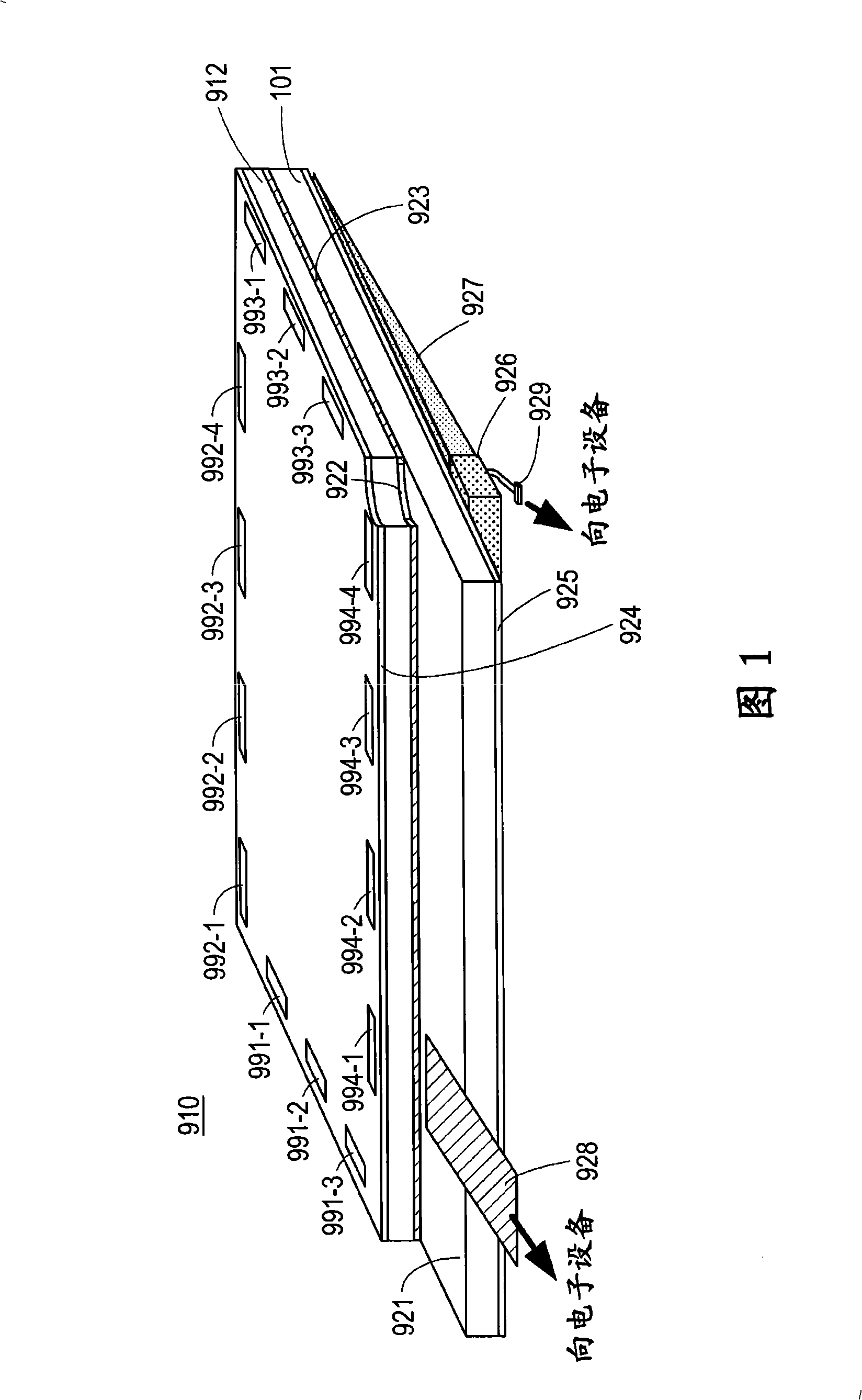
[0041] FIG. 1 is a perspective structural view (partial sectional view) of a liquid crystal display device 910 of this embodiment. The liquid crystal display device 910 is configured such that the active matrix substrate 101 and the counter substrate 912 are bonded together at a constant interval through a sealing material 923 , and a nematic liquid crystal material 922 is sandwiched between them. An alignment material made of polyimide or the like is coated on the active matrix substrate 101 and rubbed to form an alignment film (not shown). In addition, the opposite substrate 912 is formed with: a color filter (not shown) corresponding to the pixel, a black matrix 940 made of low-reflection and low-transmittance resin for preventing light leakage and improving contrast, and a The counter electrode 930 formed of an ITO film and used as a common electrode short-circuits the counter conductive portion 330 ( 330 - 1 , 330 - 2 ) on the source matrix substrate 101 . Coating an ali...
no. 2 Embodiment approach
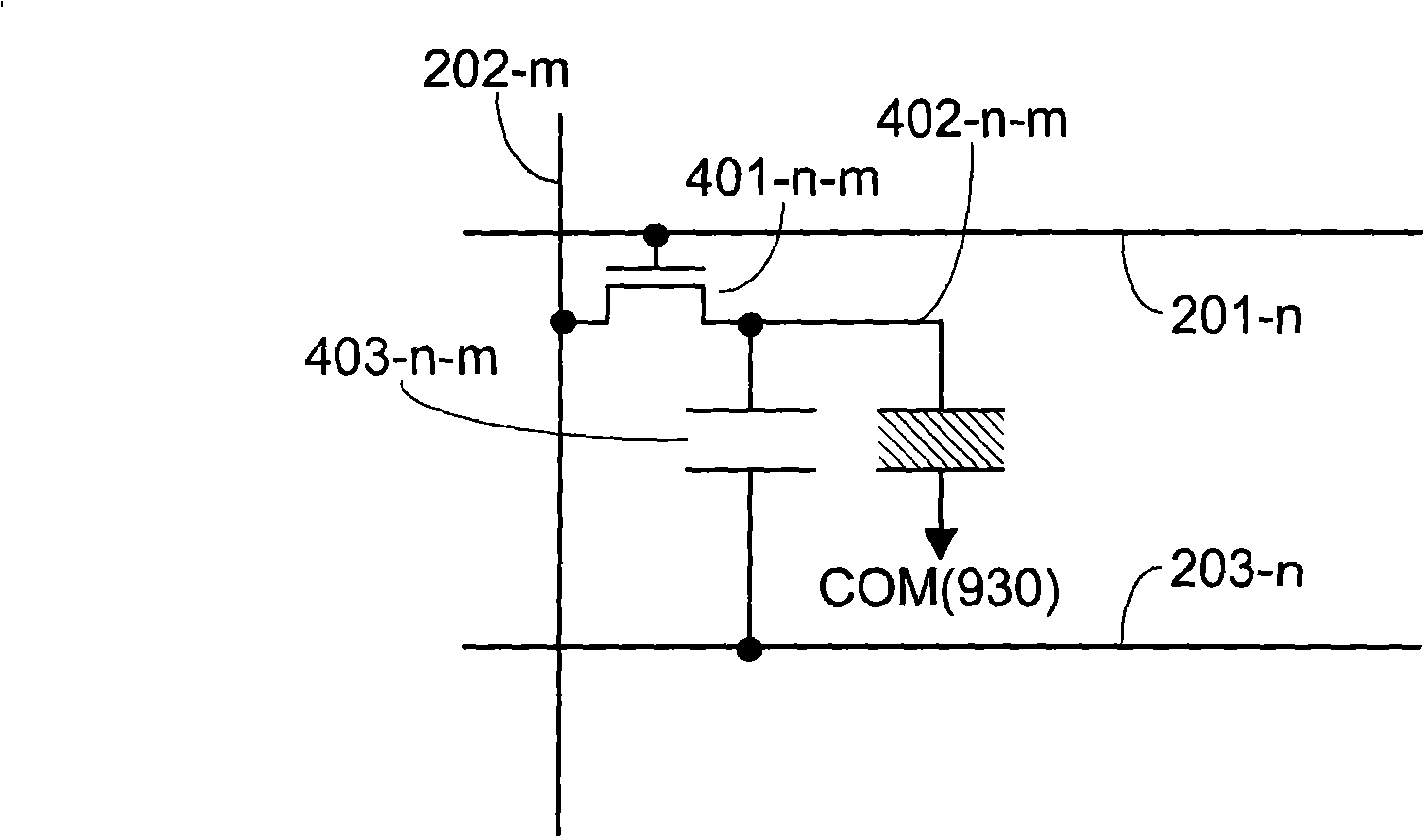
[0086] FIG. 16 is an enlarged plan view of the nth first edge light sensor 351-n as one sensor in the first edge light sensor group in the second embodiment, corresponding to FIG. 8 of the first embodiment. legend with Figure 5 same. Hereinafter, FIG. 16 will be described focusing on differences from FIG. 8 .
[0087] In Fig. 16, different from Fig. 8, the scanning line 201-n is formed of a wiring formed by an aluminum neodymium alloy film (AlNd) through a contact hole in the region overlapping with the light-shielding electrode 611-n in plan view, and the scanning line 201-n is connected to the light-shielding electrode 611-n. A common potential branch wiring 618-n made of a molybdenum thin film (Mo) is formed between the electrodes 611-n. The common potential branch wiring 618-n is connected to the common potential wiring 335 through a contact hole, and is supplied with a common potential (COM). In other respects, FIG. 16 is not different from FIG. 8 , so the same refere...
no. 3 Embodiment approach
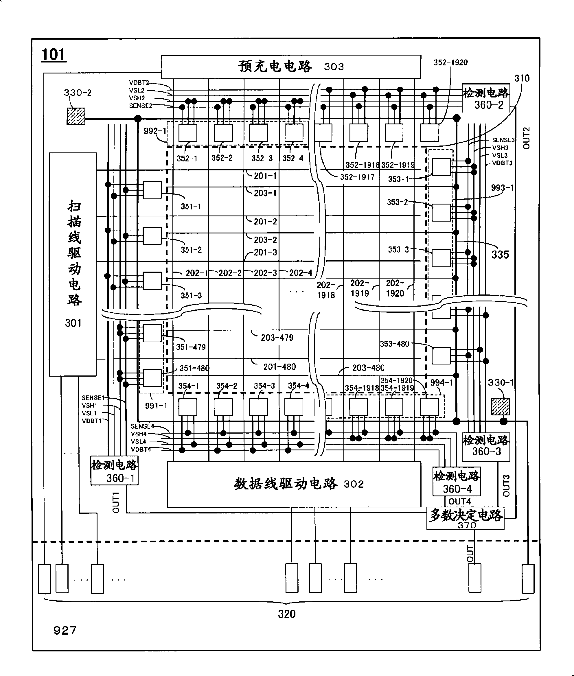
[0094] Figure 18 is a block diagram of the active matrix substrate 102 in the third embodiment, and the following is the same as that shown in the first embodiment figure 2 The difference between the active matrix substrate 101 and the first embodiment will be described. figure 2The same components are assigned the same symbols and their descriptions are omitted. In this embodiment, instead of the first edge light sensors 351-1 to 351-480 in the first embodiment, the first edge light sensors 351'-1 to 351'-480 as light sensors are arranged to replace the second edge light sensors. Sensors 352-1 to 352-1920 are equipped with second edge light sensors 352'-1 to 352'-1920 as light sensors, and third edge light sensors as light sensors are arranged instead of third edge light sensors 353-1 to 353-480 Sensors 353'-1 to 353'-480, instead of the fourth side light sensors 354-1 to 354-1920, the fourth side light sensors 354'-1 to 354'-1920 as light sensors are arranged as light sen...
PUM
 Abstract
Description
Claims
Application Information
 - R&D Engineer
- R&D Manager
- IP Professional
- Industry Leading Data Capabilities
- Powerful AI technology
- Patent DNA Extraction
Browse by: Latest US Patents, China's latest patents, Technical Efficacy Thesaurus, Application Domain, Technology Topic, Popular Technical Reports.
© 2024 PatSnap. All rights reserved.Legal|Privacy policy|Modern Slavery Act Transparency Statement|Sitemap|About US| Contact US: help@patsnap.com