


Quick Research
Generate reliable direction feasibility study reports for your R&D in just a few steps.

Technical Q&A
Discover and master advanced knowledge NOW. Basics, ideas, possibilities, all at once.

Find Solutions
As an expert in R&D theories, this can generate solutions to your technical problems instantly.

Evaluate Feasibility
Analyze your overall solution with one click, know your potential R&D risks in advance.

Monitor Landscape
Get weekly tech updates, stay abreast of the latest tech innovations and key insights.
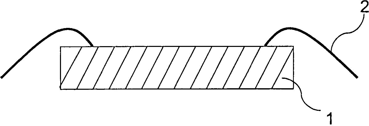
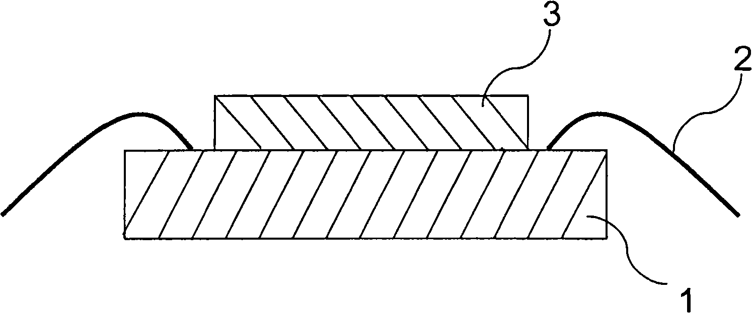
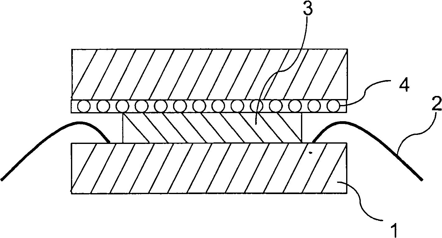
Adhesive film for stacking semiconductor chip
A technology of adhesive film and semiconductor, applied in the direction of film/sheet adhesive, semiconductor device, semiconductor/solid device manufacturing, etc., can solve the problem that it is impossible to stack 3 or more layers of chips Problems such as the same integration and inability to achieve stacking
- Summary
- Abstract
- Description
- Claims
- Application Information
AI Technical Summary
Problems solved by technology
Method used
Image

Examples
Embodiment approach
[0063] Sample 1: Making the first and third adhesive layers of epoxy
[0064] First, 100 parts by weight of cresol novolak epoxy resin (YDCN8P, commercially available from Toto Kasei Co.), 50 parts by weight of phenol novolac resin (KPH2000, commercially available from Kolon Chemical Co.), 0.02 parts by weight of 1 - a mixture of cyanoethyl-2-phenylimidazole (CURESOL 2PZ-CN, commercially available from Shikoku Kasei Co.) for 3 hours. Subsequently, 50 parts by weight of a phenoxy resin (YP50, commercially available from Toto Kasei Co.) was added to the stirred mixture, and then the mixture was further stirred for 6 hours. The resulting stirred mixture was spread on a substrate of release-treated polyethylene terephthalate film to a thickness of 38 μm. The coated film was then dried at 90° C. for 3 minutes to produce a B-staged 40 μm thick first adhesive layer and a B-staged 10 μm thick third adhesive layer.
[0065] Sample 2: Making a Second Adhesive Layer of Phenoxy Resi...
PUM
| Property | Measurement | Unit |
|---|---|---|
| tensile modulus | aaaaa | aaaaa |
| softening point | aaaaa | aaaaa |
| glass transition temperature | aaaaa | aaaaa |
Abstract
Description
Claims
Application Information
 - R&D Engineer
- R&D Manager
- IP Professional
- Industry Leading Data Capabilities
- Powerful AI technology
- Patent DNA Extraction
Browse by: Latest US Patents, China's latest patents, Technical Efficacy Thesaurus, Application Domain, Technology Topic, Popular Technical Reports.
© 2024 PatSnap. All rights reserved.Legal|Privacy policy|Modern Slavery Act Transparency Statement|Sitemap|About US| Contact US: help@patsnap.com