Semiconductor device and method of manufacturing the same
A semiconductor and conductive film technology, applied in semiconductor/solid-state device manufacturing, semiconductor devices, transistors, etc., can solve problems such as difficult control of impurity concentration, achieve suppression of short channel effects, prevent hot carrier degradation, and improve conductivity The effect of passing current
- Summary
- Abstract
- Description
- Claims
- Application Information
AI Technical Summary
Problems solved by technology
Method used
Image


Examples
Embodiment approach 1
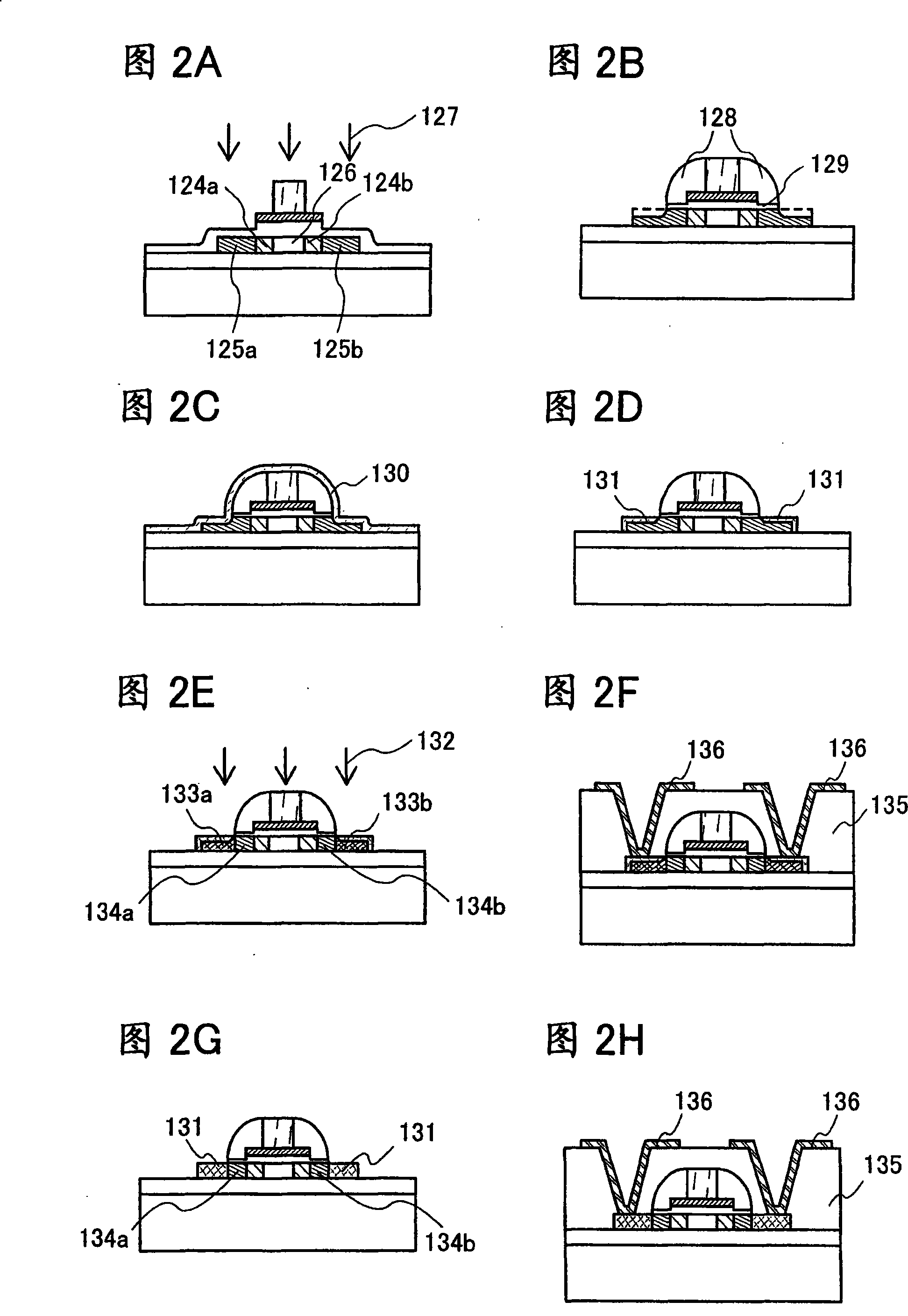
[0042] Hereinafter, a method of manufacturing a semiconductor device according to this embodiment will be described with reference to FIGS. 1A to 1D , FIGS. 2A to 2H , and FIGS. 6A and 6B .
[0043] First, base insulating film 112 is formed on substrate 111 to a thickness of 100 to 300 nm. As the substrate 111, an insulating substrate such as a glass substrate, a quartz substrate, a plastic substrate, a ceramic substrate, or the like; a metal substrate; a semiconductor substrate, or the like can be used.
[0044]As the base insulating film 112, silicon oxide (SiOx), silicon nitride (SiNx), silicon oxide containing nitrogen (SiOxNy) (x>y), silicon nitride containing oxygen (SiNxOy) (x>y) can be used. A single-layer structure of an insulating film containing oxygen or nitrogen, or a laminated structure thereof. In particular, when there is concern about contamination from the substrate, it is preferable to form a base insulating film.
[0045] In addition, when the base insula...
Embodiment approach 2
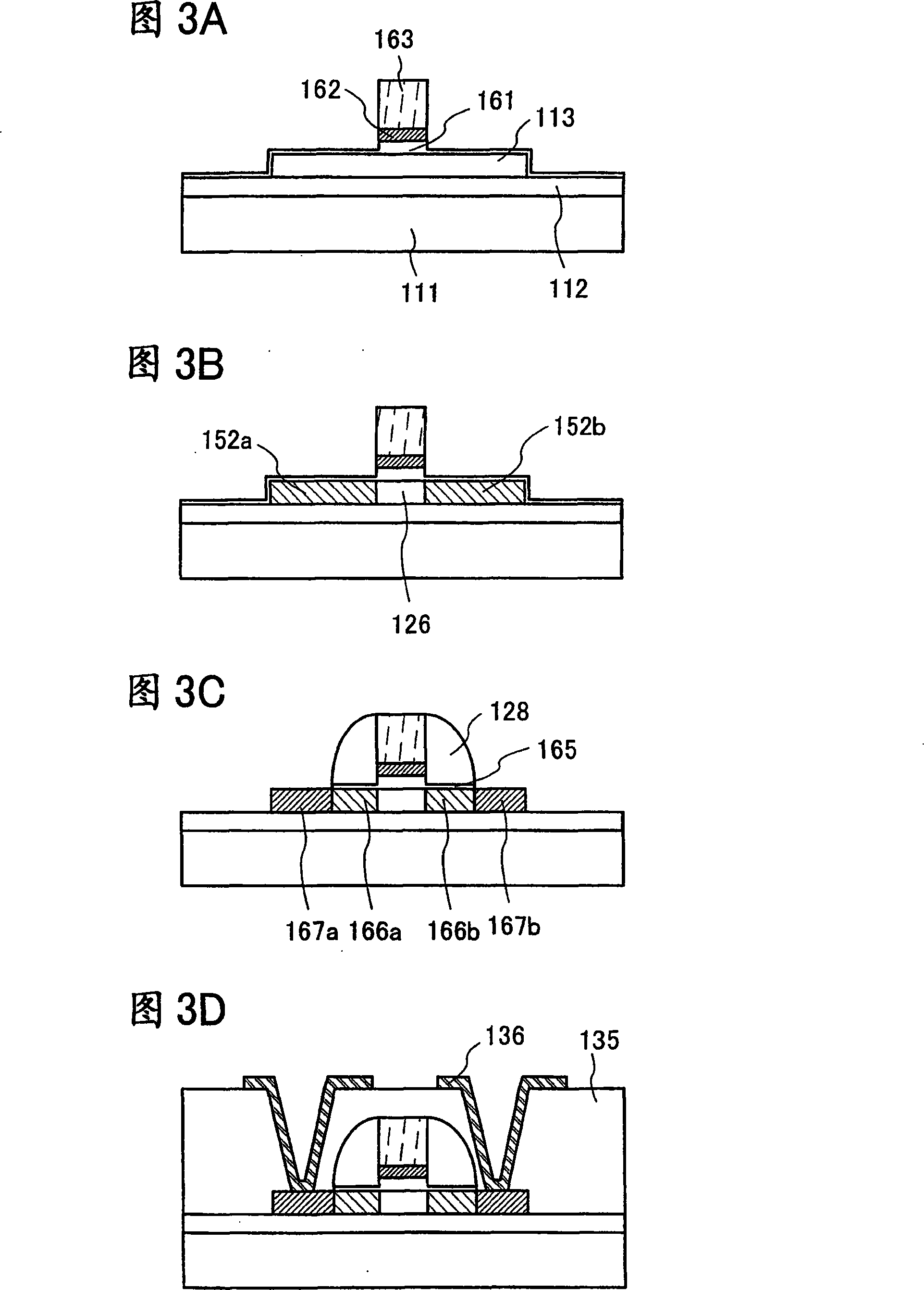
[0090] In this embodiment mode, a method of manufacturing a semiconductor device having only the Loff region is shown using FIGS. 3A to 3D . In addition, in this embodiment, the same code|symbol is used for the same part as Embodiment 1, and detailed description is abbreviate|omitted.
[0091] The structure in FIG. 1C is obtained by performing the same steps as in Embodiment Mode 1 to the second etching (see FIG. 3A ). However, in FIG. 3A , a base insulating film 112 , an island-shaped semiconductor film 113 , a gate insulating film 161 , a first gate electrode 162 , and a second gate electrode 163 are formed over a substrate 111 . In this embodiment, the width of the first gate electrode 162 is the same as that of the second gate electrode 163 . In addition, the second gate electrode 163 may or may not have a tapered angle.
[0092] The gate insulating film 161 is thinner than the film thickness of the region under the first gate electrode 162 and the second gate electrode ...
Embodiment approach 3
[0099] In this embodiment mode, a method of manufacturing a semiconductor device having only the Loff region, which is different from the second embodiment mode, is shown using FIGS. 4A to 5D . In addition, in this embodiment, the same code|symbol is used for the same part as Embodiment 1 and Embodiment 2, and detailed description is abbreviate|omitted.
[0100] First, the structure of FIG. 3C is obtained in the same manner as in Embodiment 2 (see FIG. 4A ). In other words, the base insulating film 112 , the island-shaped semiconductor film 113 , the gate insulating film 161 , the first gate electrode 162 , and the second gate electrode 163 are formed on the substrate 111 . A channel formation region 126 and low-concentration impurity regions 152 a and 152 b are formed in the island-shaped semiconductor film 113 .
[0101] The gate insulating film 161 is thinner than the film thickness of the region under the first gate electrode 162 and the second gate electrode 163 , except...
PUM
| Property | Measurement | Unit |
|---|---|---|
| length | aaaaa | aaaaa |
| particle diameter | aaaaa | aaaaa |
Abstract
Description
Claims
Application Information
 - R&D
- Intellectual Property
- Life Sciences
- Materials
- Tech Scout
- Unparalleled Data Quality
- Higher Quality Content
- 60% Fewer Hallucinations
Browse by: Latest US Patents, China's latest patents, Technical Efficacy Thesaurus, Application Domain, Technology Topic, Popular Technical Reports.
© 2025 PatSnap. All rights reserved.Legal|Privacy policy|Modern Slavery Act Transparency Statement|Sitemap|About US| Contact US: help@patsnap.com