Display device and flat display device
A display device, planar technology, applied in lighting devices, printed circuits, instruments, etc., can solve problems such as uneven connection of terminals, achieve uniform thermal curing conditions, reduce bending stress concentration, and increase reliability.
- Summary
- Abstract
- Description
- Claims
- Application Information
AI Technical Summary
Problems solved by technology
Method used
Image

Examples
Embodiment 1
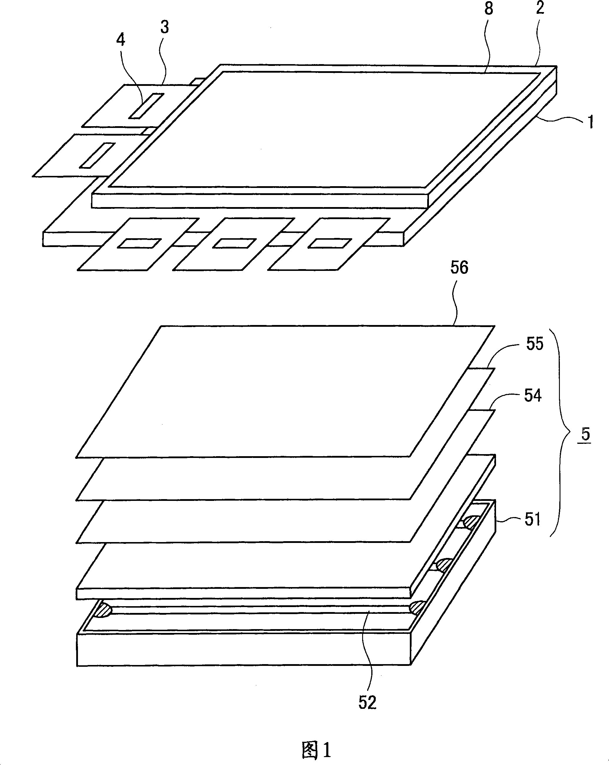
[0069] FIG. 1 is a liquid crystal display module for TV as an example of implementing the present invention. In FIG. 1 , a TFT substrate 1 on which pixel electrodes, thin film transistors, and the like are arranged in a matrix and a color filter substrate 2 on which color filters are formed in a matrix are stacked. The TFT substrate 1 is made larger than the color filter substrate 2 in order to provide the COF 3 and the like on the TFT substrate. COF is an abbreviation for chip-on-film package, but this specification sometimes uses the meaning of COF film. Liquid crystal is interposed between the TFT substrate 1 and the color filter substrate 2 . An upper polarizing plate 8 is attached to the color filter substrate 2 , and a lower polarizing plate (not shown) is attached to the lower surface of the TFT substrate 1 . On both sides of the TFT substrate 1, a COF on which an IC chip 4 including a driving circuit is mounted is provided. In Fig. 1, three COFs are installed on the...
Embodiment 2
[0096] In the first embodiment, a plurality of branch positions of the thick wiring is provided, and the branch positions are regularly changed for each line. Example 2 is a case where the branch positions are continuously changed for each adjacent thin wiring. In FIG. 13 , each thick wiring branch on the COF is two thin wirings. The positions of the branches are gradually separated from the TFT substrate side terminal 34 of the COF such that the wiring P1 is at the position A, the wiring P2 is at the position B, and the wiring P3 is at the position C. In this way, by dispersing the positions of the branches, it is possible to disperse the bending stress when bending the COF 3 .
[0097] FIG. 13 is an example of continuously changing the positions where thick lines of the same width branch into thin lines, but the continuous change of branch positions is not limited to lines of the same width. FIG. 14 is an example of changing the branch position when wirings having differen...
Embodiment 3
[0102] On the COF, straight wiring is rarely possible from the TFT substrate-side terminal 34 of the COF to the printed wiring board-side terminal 35 of the COF, and the wiring is usually bent on the way. In addition, when the wiring is bent, the width of the line may also change at the same time. There are various methods of bending the wiring in this case. The simplest method is the one shown in Figure 16. FIG. 16 shows a case where the width of the wiring is changed to w2 after the wiring having the width w1 is bent. In FIG. 16, the thin wiring before bending is constant at w1. In addition, the thick wiring after bending is also constant at w2. However, in this case, since the thickness of the wiring changes rapidly at the bent portion, when the COF 3 is bent, disconnection is likely to occur at the bent portion of the wiring, for example, the portion B in FIG. 16 . This embodiment is an example of preventing disconnection at such bent wiring portions.
[0103] FIG. 17...
PUM
 Abstract
Description
Claims
Application Information
 - Generate Ideas
- Intellectual Property
- Life Sciences
- Materials
- Tech Scout
- Unparalleled Data Quality
- Higher Quality Content
- 60% Fewer Hallucinations
Browse by: Latest US Patents, China's latest patents, Technical Efficacy Thesaurus, Application Domain, Technology Topic, Popular Technical Reports.
© 2025 PatSnap. All rights reserved.Legal|Privacy policy|Modern Slavery Act Transparency Statement|Sitemap|About US| Contact US: help@patsnap.com