Circuit board information acquisition and conversion method, program, and device for the same
A conversion method and conversion device technology, applied in the direction of circuit heating device, circuit, printed circuit, etc., can solve the problems of improving analysis accuracy, not being able to simplify the analysis model, shortening the analysis time, etc., and achieve the effect of reducing the scale
- Summary
- Abstract
- Description
- Claims
- Application Information
AI Technical Summary
Problems solved by technology
Method used
Image
Examples
example 1
[0094] Fig. 5 is a block diagram showing the configuration of a circuit board information acquisition and conversion device.
[0095] The circuit board information acquisition and conversion device 51 includes a circuit board design information input unit 52, a library 53, an analysis / conversion / processing unit 54 and a simulation unit 55.
[0096] The circuit board design information input unit 52 acquires circuit board design information (circuit board design data) generated based on the circuit diagram data input by the operator when designing the circuit board. Then, the circuit board design information is transferred to the analysis / conversion / processing unit 54. In this configuration, necessary information can also be obtained from the library 53 because in some cases, the wiring trace or the shape of the through hole is not included in the circuit board design information.
[0097] The library 53 is a memory. In the library 53, the characteristic information corresponding t...
example 2
[0125] Next, the circuit board simplification based on heat generation density will be explained.
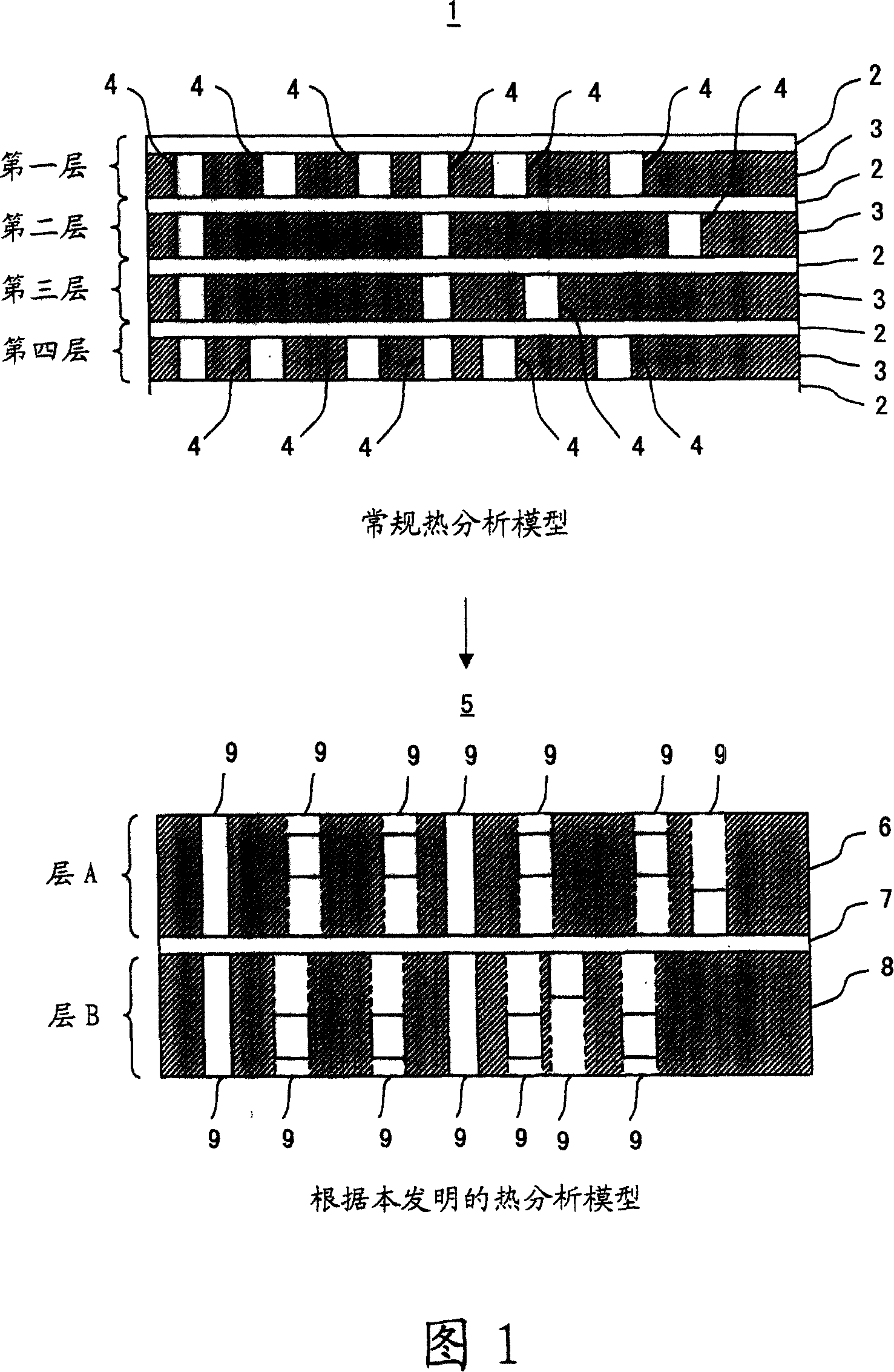
[0126] FIG. 9 shows an example in which, based on the heat generation density calculated from the package area and the heat generation amount, a through hole is modeled as an analysis model for a mounting component whose heat generation density makes it vulnerable to thermal damage.
[0127] The analysis / conversion / processing unit 54 additionally includes a heat generation density determination unit, and a predetermined heat generation density determination value is recorded in a memory (bank 53 etc.).
[0128] Based on the heat generation amount of each mounted component, the heat generation density determination unit calculates the heat generation density that affects the vicinity of the components on the circuit board. Compare the calculated heating density and the determined value of heating density with each other. When the calculated heating density is equal to or greater than...
example 3
[0134] In Example 3, the heat generation density distribution of the analysis model is explored according to the circuit board design information, and the through holes are arranged in areas with large heat generation density or extremely different heat density, and no through holes are provided in other areas.
[0135] Similar to Example 2, a heat generation density determination unit for calculating heat generation density is provided. In addition, the analysis / conversion / processing unit 54 is provided with a region setting unit and the like, and the region as shown in FIG. 10 is determined (region setting processing). The area is divided on the board as shown by the dotted line. In this example, the area is square, but the scope of the present invention is not limited to this shape. In addition, the area may be determined based on the operator's selection.
[0136] In each area, the heating density calculated by the heating density determination unit is compared with the heatin...
PUM
 Abstract
Description
Claims
Application Information
 - R&D Engineer
- R&D Manager
- IP Professional
- Industry Leading Data Capabilities
- Powerful AI technology
- Patent DNA Extraction
Browse by: Latest US Patents, China's latest patents, Technical Efficacy Thesaurus, Application Domain, Technology Topic, Popular Technical Reports.
© 2024 PatSnap. All rights reserved.Legal|Privacy policy|Modern Slavery Act Transparency Statement|Sitemap|About US| Contact US: help@patsnap.com


