


Quick Research
Generate reliable direction feasibility study reports for your R&D in just a few steps.

Technical Q&A
Discover and master advanced knowledge NOW. Basics, ideas, possibilities, all at once.

Find Solutions
As an expert in R&D theories, this can generate solutions to your technical problems instantly.

Evaluate Feasibility
Analyze your overall solution with one click, know your potential R&D risks in advance.

Monitor Landscape
Get weekly tech updates, stay abreast of the latest tech innovations and key insights.
Electric field-tunable negative magnetic permeability part based on ferroelectric ceramic grain and its making method
A technology of ferroelectric ceramics and negative magnetic permeability, which is applied in the direction of waveguide devices, electrical components, circuits, etc., and can solve the problems of limited application range, expensive, and complex geometric shapes of metal structural units
- Summary
- Abstract
- Description
- Claims
- Application Information
AI Technical Summary
Problems solved by technology
Method used
Image

Examples
Embodiment 1
[0047] Preparation of Ba by solid-phase reaction synthesis 0.5 Sr 0.5 TiO 3 (BST) powder. The method uses high-purity BaCO 3 , SrCO 3 and TiO 2 As a raw material, react with the following equation to obtain Ba 0.5 Sr 0.5 TiO 3 Powder.
[0048] 0.5BaCO 3 +0.5SrCO 3 +TiO 2 = Ba 0.5 Sr 0.5 TiO 3 +CO 2 ↑
[0049] BaCO 3 , SrCO 3 and TiO 2 Mix according to the above proportions, after ball milling, drying and sieving, calcining at 1150°C for 3 hours, then ball milling and drying to obtain BST powder for use.
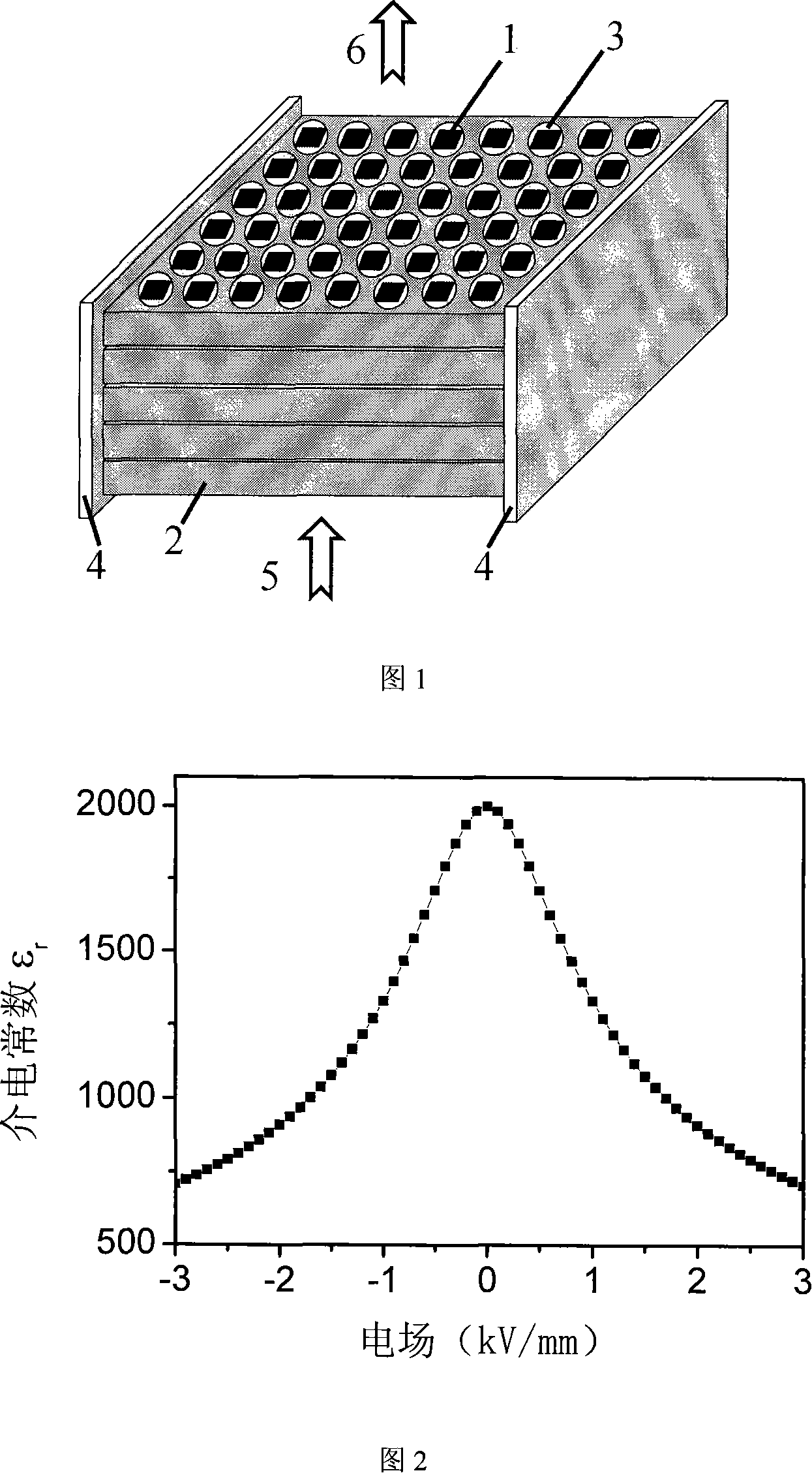
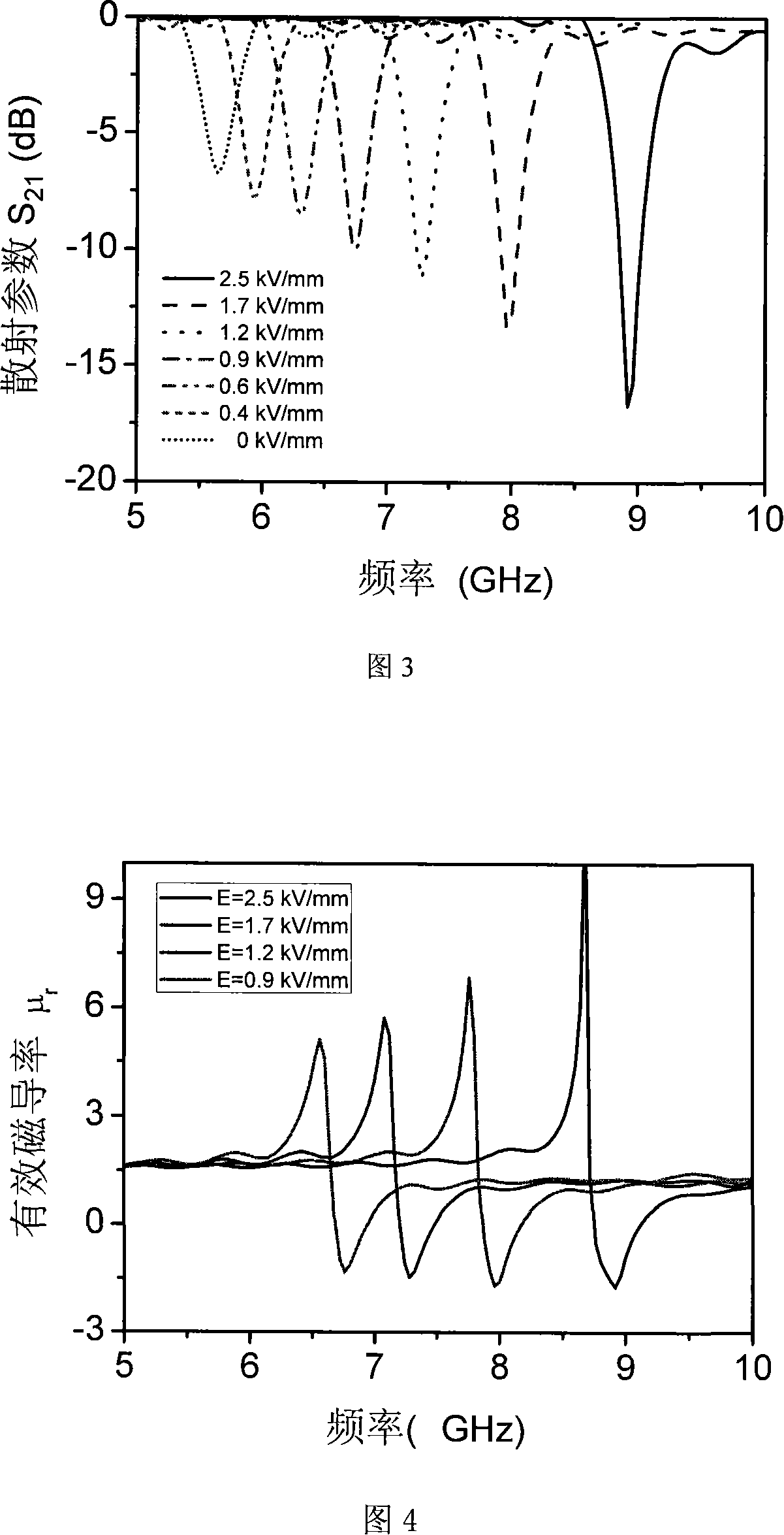
[0050] Using the ceramic slurry casting technology, the BST powder and organic solvent are made into a slurry for casting to obtain a cast sheet with a thickness of 1.25mm, and then the cast sheet is cut into cubes with a side length of 1.25mm and processed at 300 ℃ for debinding, and finally sintered at 1350 ℃ for 3 hours to obtain a ferroelectric ceramic cube with a side length of 1.0 mm. The relationship curve of its dielectric properties with the appl...
Embodiment 2
[0054] With embodiment one, utilize solid phase reaction synthesis method to prepare Ba 0.5 Sr 0.5 TiO 3 (BST) powder, using ceramic slurry casting technology to cast and discharge glue, sintering to obtain BST ceramic cubes with a side length of 0.70mm. The relationship curve of its dielectric properties with the applied electric field is shown in Figure 2. It can be seen that its relative permittivity at room temperature and zero field is 2000.
[0055] A circular hole array with a diameter of 1.00 mm is drilled on a polytetrafluoroethylene plate with a thickness of 2.50 mm by using a numerical control machine tool. The ceramic cubes were embedded into the round holes of the polytetrafluoroethylene template to produce a two-dimensional array of ceramic cubes. Then align the round holes of the polytetrafluoroethylene plates embedded with ceramic cubes to perform lamination and bonding to obtain a three-dimensional ceramic cube array.
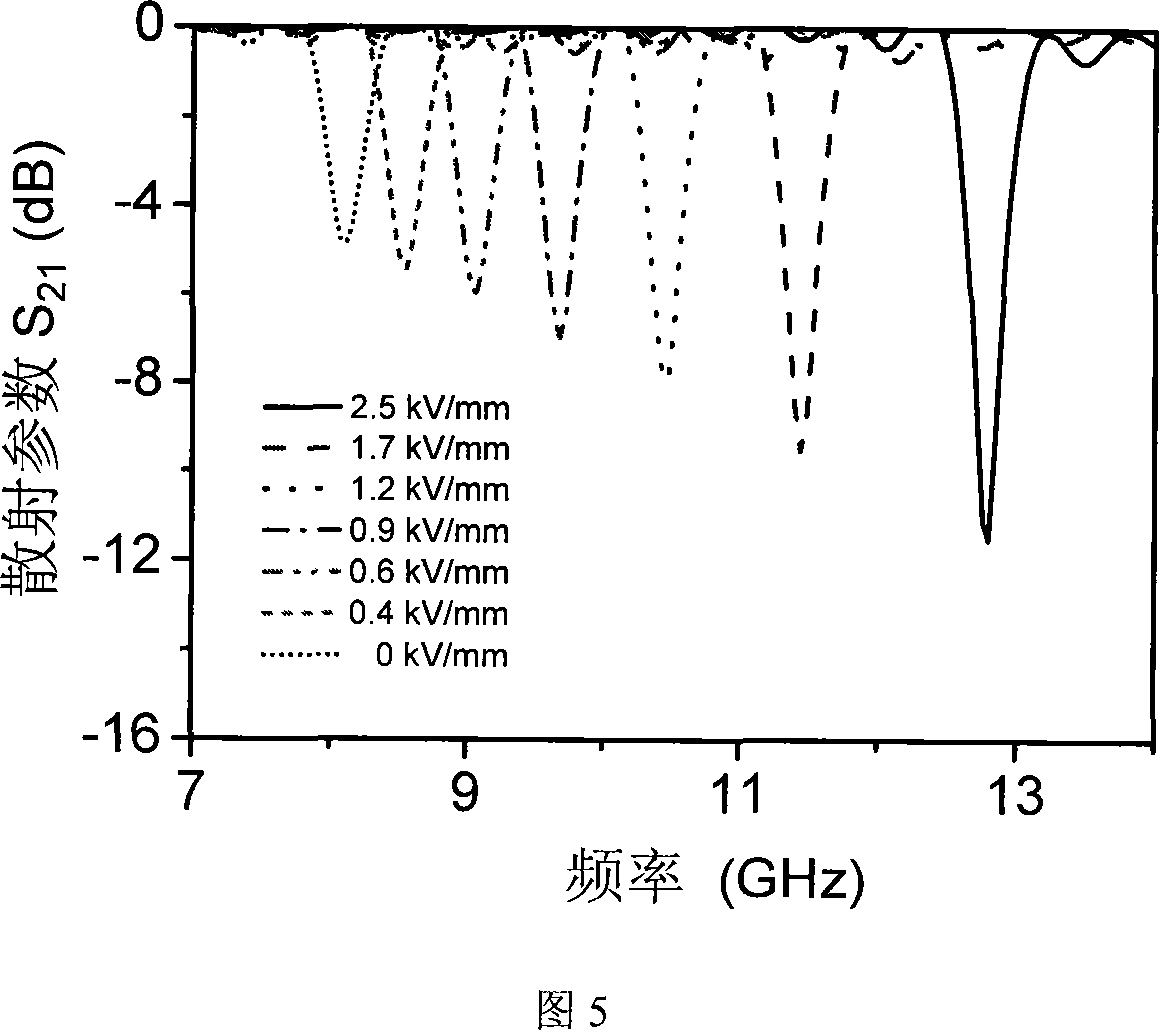
[0056] The electric field tunable ne...
Embodiment 3
[0058] With embodiment one, utilize solid phase reaction synthesis method to prepare Ba 0.4 Sr 0.6 TiO 3 (BST) powder, mix BST powder with 5wt% MgO powder and mix with organic solvent to form a slurry for casting to make a casting sheet with a thickness of 0.57mm, then debinding and sintering to obtain the side length A ceramic cube of 0.45mm has a relative permittivity of 1600 at room temperature and zero field.
[0059] A circular hole array with a diameter of 0.64 mm is drilled on a polytetrafluoroethylene plate with a thickness of 1.00 mm by using a numerical control machine tool. The ceramic cubes were embedded into the round holes of the polytetrafluoroethylene template to produce a two-dimensional array of ceramic cubes. Then align the round holes of the polytetrafluoroethylene plates embedded with ceramic cubes to perform lamination and bonding to obtain a three-dimensional ceramic cube array.
[0060] Finally, the three-dimensional ceramic cube array is bonded tog...
PUM
| Property | Measurement | Unit |
|---|---|---|
| Lattice constant | aaaaa | aaaaa |
| Side length | aaaaa | aaaaa |
| Diameter | aaaaa | aaaaa |
Abstract
Description
Claims
Application Information
 - R&D Engineer
- R&D Manager
- IP Professional
- Industry Leading Data Capabilities
- Powerful AI technology
- Patent DNA Extraction
Browse by: Latest US Patents, China's latest patents, Technical Efficacy Thesaurus, Application Domain, Technology Topic, Popular Technical Reports.
© 2024 PatSnap. All rights reserved.Legal|Privacy policy|Modern Slavery Act Transparency Statement|Sitemap|About US| Contact US: help@patsnap.com