Semiconductor packaging structure with common type wafer holder

A chip seat and semiconductor technology, applied in the direction of semiconductor devices, semiconductor/solid device parts, electric solid devices, etc., can solve the problems of unbalanced mold flow, no structure of general products, lack of fixation around the wafer, etc., to achieve increased integration intensity effect

Inactive Publication Date: 2008-02-06
CHIPMOS TECH INC
View PDF0 Cites 8 Cited by
  • Summary
  • Abstract
  • Description
  • Claims
  • Application Information

AI Technical Summary

Problems solved by technology

When another wafer 110A with a smaller size is fixed on the wafer holder 130 of the above-mentioned same lead frame, the space above the wafer 110A becomes smaller and the obstacle factor becomes smaller, so the flow velocity of the upper mold flow 121 will be greater than the flow velocity of the lower mold flow 122 , leading to an unbalanced mold flow. Therefore, in the known conventional technology, a single type of lead frame can only carry a single-sized chip, otherwise there will be problems of insufficient filling and exposed gold wires
[0005] China Taiwan Patent Announcement No. 396557 "The method of balancing the mold flow (mold flow) of packaging IC devices" is to use a part of the pin to bend to correct the balance of the upper and lower mold flow, but the lead frame with the bent pins can only Holds single size wafers
[0006] China Taiwan Invention Patent No. I236123 "semiconductor package", it is to make the periphery of the chip seat form a plurality of stepped parts that are sunken downwards, and these stepped parts are supported on the lower mold when pressing the mold, so as to avoid The tipping of the wafer seat occurs during the glue injection, which solves the problem of exposed gold lines. Although the size of the wafer can be slightly changed, the problem of unbalanced upper and lower mold flow still exists, so there will be situations where the filling is not full.
In addition, the supporting point of the stepped part will be exposed on the bottom surface of the molding compound, which will change the appearance of the product
In addition, only the center of the large-sized chip adheres to the chip holder, and the periphery of the chip is not fixed, so there will be problems of non-sticking when bonding wires.
[0007] It can be seen that the above-mentioned existing semiconductor packaging structure obviously still has inconvenience and defects in structure and use, and needs to be further improved urgently.
In order to solve the above-mentioned problems, the relevant manufacturers have tried their best to find a solution, but for a long time no suitable design has been developed, and the general products do not have a suitable structure to solve the above-mentioned problems. This is obviously related The problem that the industry is eager to solve

Method used


Image

  • Semiconductor packaging structure with common type wafer holder
  • Semiconductor packaging structure with common type wafer holder
  • Semiconductor packaging structure with common type wafer holder

Examples


no. 1 Embodiment

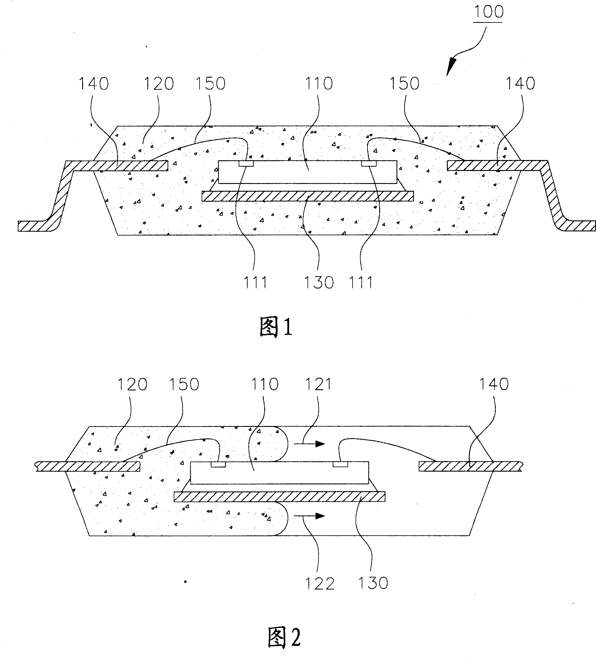
[0057] According to the first embodiment of the present invention, a semiconductor package structure with a common chip holder is disclosed, which can package chips of different sizes in the same lead frame structure without the problem of unbalanced mold flow between upper and lower molds.

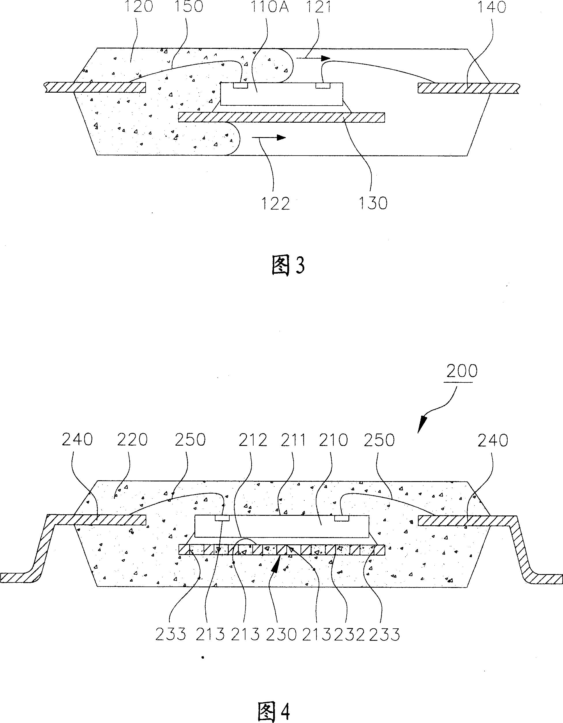
[0058] Please refer to FIG. 4 and FIG. 5. FIG. 4 is a schematic cross-sectional view of a semiconductor package structure with a shared wafer seat according to the first specific embodiment of the present invention. FIG. 5 is a schematic cross-sectional view according to the first specific implementation of the present invention. For example, the schematic diagram of the lead frame of the semiconductor package structure. As shown in FIG. 4 , a semiconductor package structure 200 with a common chip holder mainly includes a lead frame, a chip 210 and a molding compound 220 .

[0059] Please refer to FIG. 5, the above-mentioned lead frame has a shared chip holder 230 and a plurality of pins ...

no. 2 Embodiment

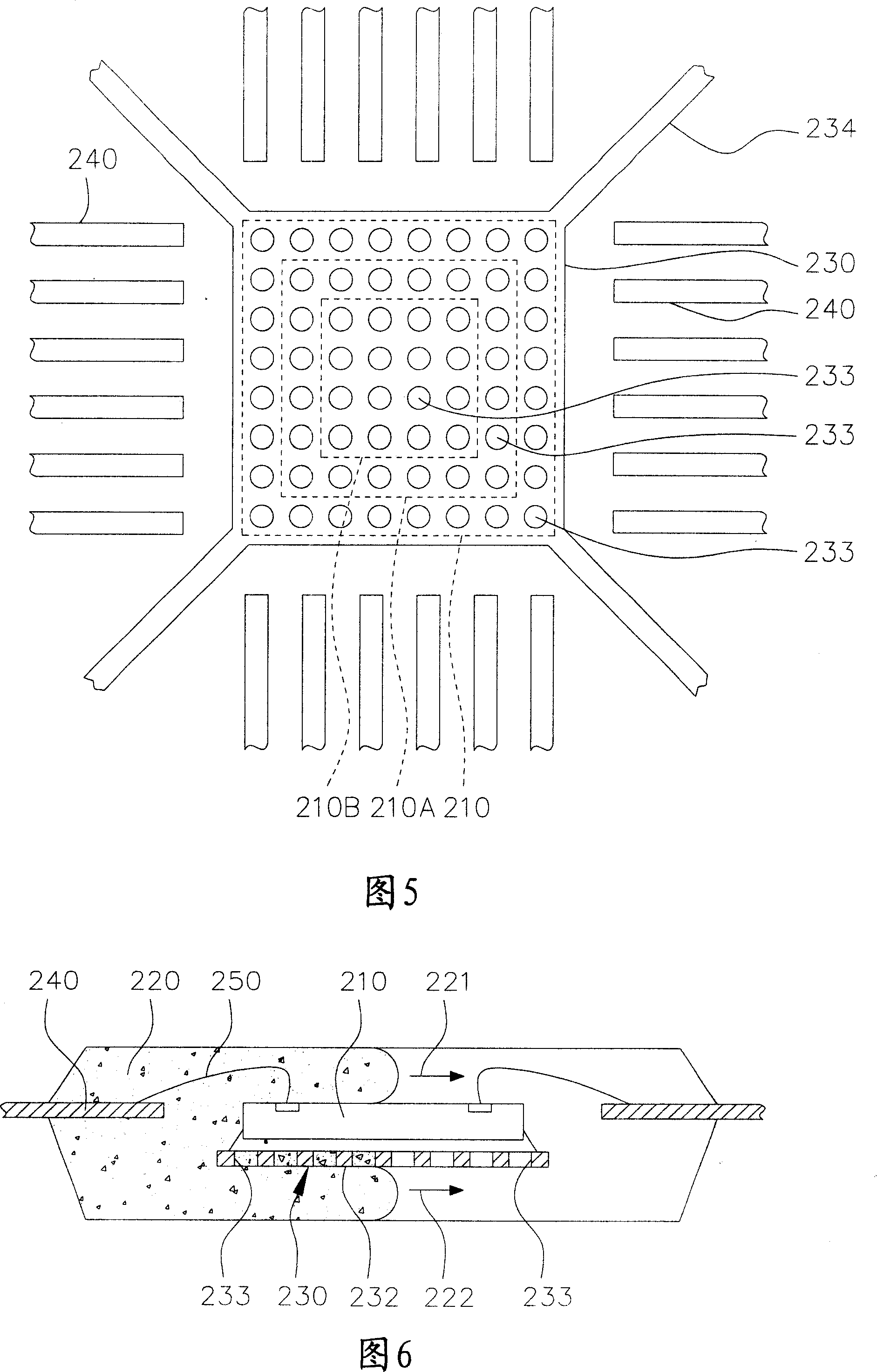
[0066] Please refer to FIG. 10 , which is a schematic diagram of a lead frame of the semiconductor package structure according to a second embodiment of the present invention. In this embodiment, the mold flow bypass holes 333 pass through the upper surface 331 and the lower surface 332 and are formed on the periphery of the shared chip holder 330. In the process, in addition to forming the mold flow bypass holes 333 in stamping, a plurality of selective mold flow bypass holes 333A can be formed on the shared wafer holder 330 at the same time, so that the shared wafer holder 330 330 has mold flow bypass holes arranged in a peripheral arrangement or in a matrix arrangement. The chip 310 is disposed on the upper surface 331 of the shared chip holder 330 , and the plurality of bonding pads 311 of the chip 310 are electrically connected to the pins 340 through a plurality of bonding wires 350 . The molding compound 320 covers the chip 310 and the bonding wires 350 .

[0067] Sin...


PUM


Abstract

The present invention relates to a semiconductor packaging structure with a common wafer bearing seat. A lead frame has the common wafer bearing seat and a plurality of pins. The common wafer bearing seat has a plurality of mould flow through holes communicating with each other upwards and downwards, which can be arranged in an array or arranged around the circumference. The wafers with different size can be installed on the common wafer bearing seat, and is wrapped with a mould sealing glue body. The number for the mould flow through holes uncovered by the wafer or the communication area also can be increased following the contract changing for the size of the wafer, which makes the upper mould flow or lower mould flow with higher flow speed having separated flowing effect, so the installing on the same guide line frame for the wafer with different size can reach the balance for the upper and lower mould flows.

Description

technical field [0001] The invention relates to a semiconductor package technology for balancing mold flow for chips with different sizes in the same lead frame structure, in particular to a semiconductor package structure with a common chip seat. Background technique [0002] In the conventional TSOP and TQFP semiconductor packaging fields, a die pad of a lead frame is used to fix a semiconductor chip and electrically connect the chip to the pins of the lead frame. Finally, mold compound is used to cover and protect the chip. During the mold forming process of the molding colloid, there will be problems of insufficient filling or exposed gold lines due to the difference in the flow rate of the upper and lower mold flows. Therefore, according to the different size changes of the wafer, different lead frames are designed according to the mold flow simulation model to achieve a balance between the upper and lower mold flows. However, the increase in the material types of the ...

Claims


Application Information

Patent Timeline
IPC IPC(8): H01L23/495H01L23/28
CPCH01L2224/83385H01L2224/32245H01L2224/48091H01L2224/48247H01L2224/73265H01L2924/181H01L2924/00014H01L2924/00H01L2924/00012
Inventor 林鸿村
Owner CHIPMOS TECH INC
Why Eureka
Try Eureka