Glass crystal packaging structure for image sensory element

An image sensor and glass flip-chip technology, which is applied in the direction of electric solid-state devices, semiconductor devices, semiconductor/solid-state device components, etc., to achieve large deformation and ensure the effect of dispensing effect.

Inactive Publication Date: 2008-02-06
CHIPMOS TECH INC
View PDF0 Cites 7 Cited by
  • Summary
  • Abstract
  • Description
  • Claims
  • Application Information

AI Technical Summary

Problems solved by technology

[0006] The main purpose of the present invention is to overcome the defects of the existing chip-on-glass package structure of the image sensor and provide a new chip-on-glass package structure of the image sensor. The technical problem to be solved is to make the When the deformable bumps are bonded to the connection pads of the glass substrate, the gap between the image sensor chip and the glass substrate can be narrowed, so that the airtight stop ring is more likely to block the light that flows into the image sensor chip from a bit of glue The sensing area can ensure the dispensing effect of the image sensor, which is very suitable for practical

Method used


Image

  • Glass crystal packaging structure for image sensory element
  • Glass crystal packaging structure for image sensory element
  • Glass crystal packaging structure for image sensory element

Examples


Embodiment Construction

[0046] In order to further explain the technical means and effects adopted by the present invention to achieve the intended purpose of the invention, the specific implementation methods, Structure, characteristic and effect thereof are as follows in detail.

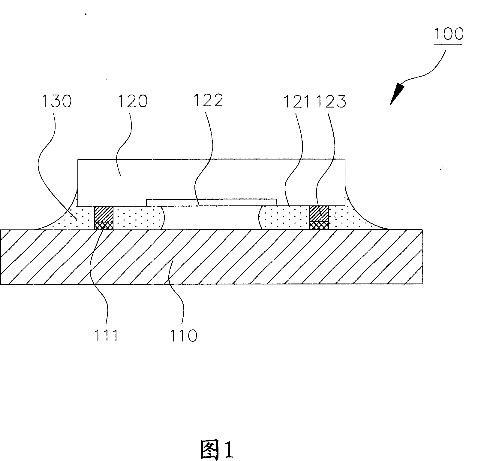
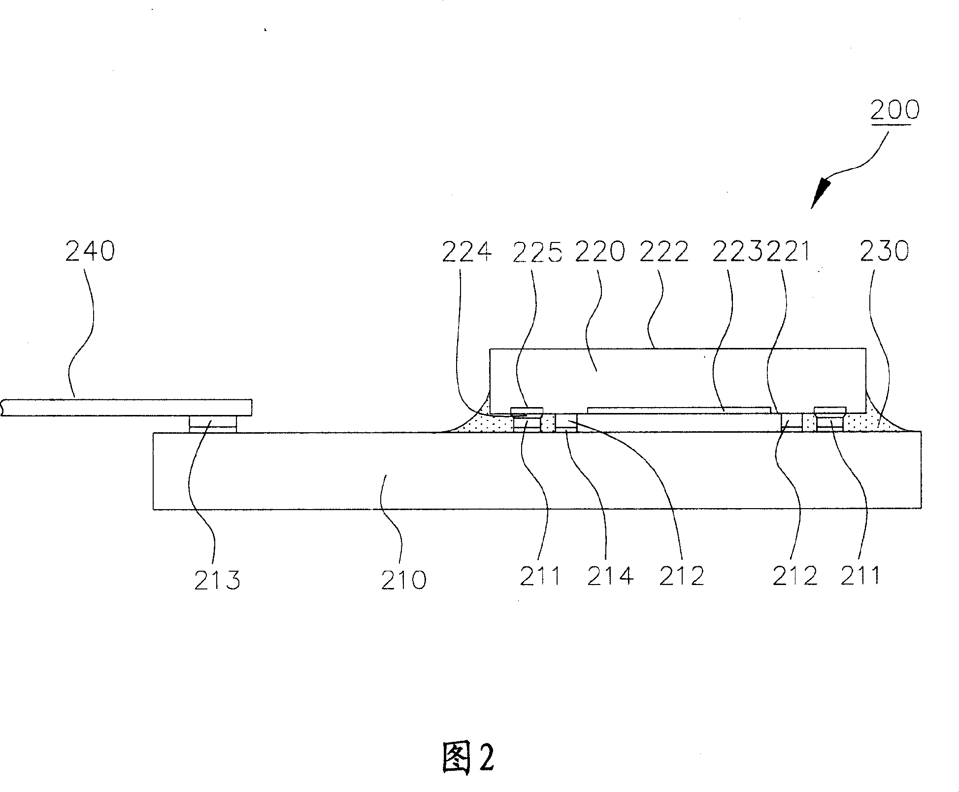
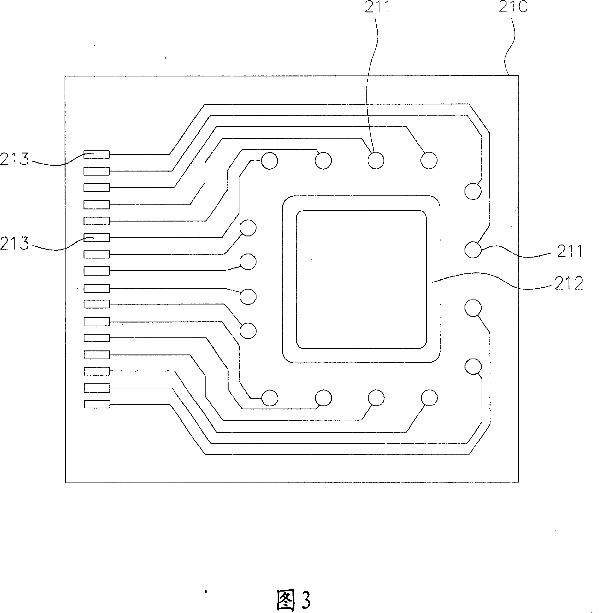
[0047] According to a first embodiment of the present invention, please refer to FIG. 2 to FIG. 4 , which discloses a chip-on-glass packaging structure of an image sensor. Please refer to FIG. 2 , which is a schematic cross-sectional view of a chip-on-glass package structure of an image sensor according to a specific embodiment of the present invention. The chip-on-glass packaging structure 200 of the image sensor mainly includes a glass substrate 210 , an image sensor chip 220 and a dot-coated glue 230 . The glass substrate 210 bears the image sensor chip 220 and provides functions of telecommunication switching and light receiving path. The dispensing glue 230 partially seals the image sensor chip 220 and firmly bonds...


PUM


Abstract

The present invention relates to a glass crystal coating sealing structure for the image sensor, which mainly comprises a glass basal plate, an image sensor crystal and a point photoresist coating body. One active face of the image sensor crystal comprises a light sensing area, and the glass basal plate has a closed blocking ring around the light sensing area, and the active face of the image sensor crystal is provided with a plurality of protruding blocks which can be distorted, and when the protruding blocks which can be distorted are connected with the connecting cushion of the glass basal plate, the present invention can reduce the clearance between the image sensor crystal and the glass basal plate to make the closed blocking ring easily blocking the flowing to the light sensing area of the image sensor crystal for the point photoresist coating body, thereby ensuring having good point coating effect.

Description

technical field [0001] The invention relates to a semiconductor packaging technology for an image sensor chip, in particular to a device capable of narrowing the gap between the image sensor chip and the glass substrate, so that the airtight stop ring is more likely to prevent the dispensing glue from flowing into the image sensor The light-sensing area of ​​the sensor chip can ensure the chip-on-glass package structure (Chip-On-Glass (COG) package) of the image sensor with good dispensing effect. Background technique [0002] In the early image sensor packaging structure, the image sensor chip is glued on a printed circuit board, and the two are electrically connected by bonding wires. An optical glass is pre-attached on the active surface of the chip before packaging, or adhered to a retaining wall on the substrate after packaging, so the thickness of the entire package becomes thicker. In recent years, the packaging structure of image sensors has been tried to change to ...

Claims


Application Information

Patent Timeline
Patent Type & Authority Applications(China)
IPC IPC(8): H01L23/31H01L23/48
CPCH01L2924/0002H01L2224/16225
Inventor 黄祥铭刘安鸿李宜璋吕良田林勇志
Owner CHIPMOS TECH INC
Why Eureka
Try Eureka