Semiconductor memory module having built-in antenna
A memory module and antenna module technology, applied in semiconductor devices, semiconductor/solid-state device parts, antennas, etc., can solve the problem of not being able to fully ensure the length of the antenna, and achieve the effect of large capacity
- Summary
- Abstract
- Description
- Claims
- Application Information
AI Technical Summary
Problems solved by technology
Method used
Image
Examples
no. 1 Embodiment approach
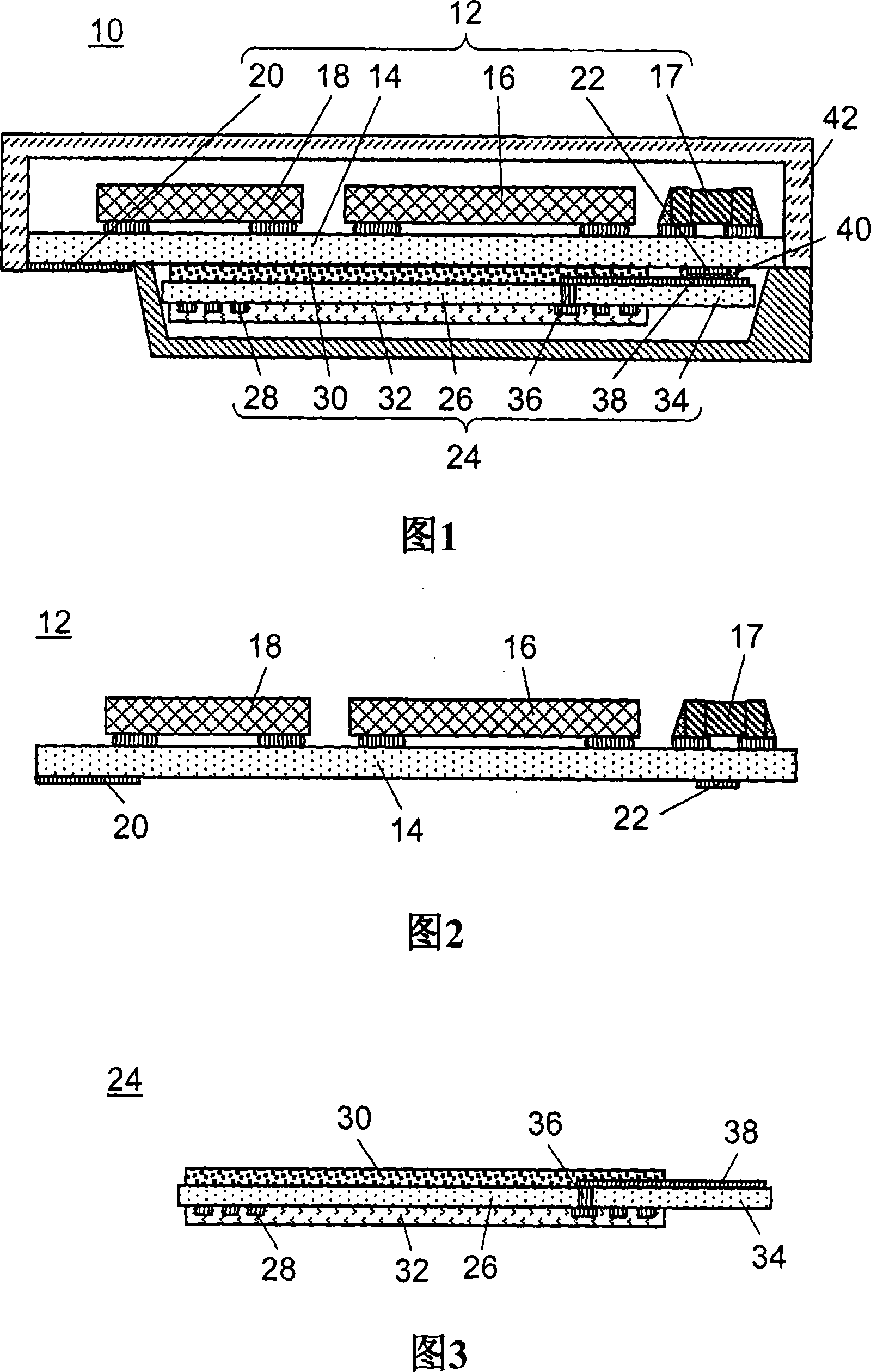
[0090] FIG. 1 is a cross-sectional view of an SD memory card 10 according to a first embodiment of the present invention. 2 is a cross-sectional view of the mounting module 12 which is one of the main parts, and FIG. 3 is a cross-sectional view of the antenna module 24 which is also one of the main parts. The SD memory card of this embodiment has a contact connection function and a non-contact information transmission function.
[0091] As shown in FIG. 1 , in the SD memory card 10 of this embodiment, the mounting module 12 and the antenna module 24 are superimposed, and the antenna connection terminal electrode (hereinafter referred to as the antenna connection terminal) 22 and the antenna terminal electrode 38 are joined, and the These are housed in the exterior case 42 . In addition, the connection terminal 20 formed on the wiring board 14 of the mounting module 12 is exposed from the surface of the exterior case 42, and this connection terminal 20 is a terminal for connec...
no. 2 Embodiment approach
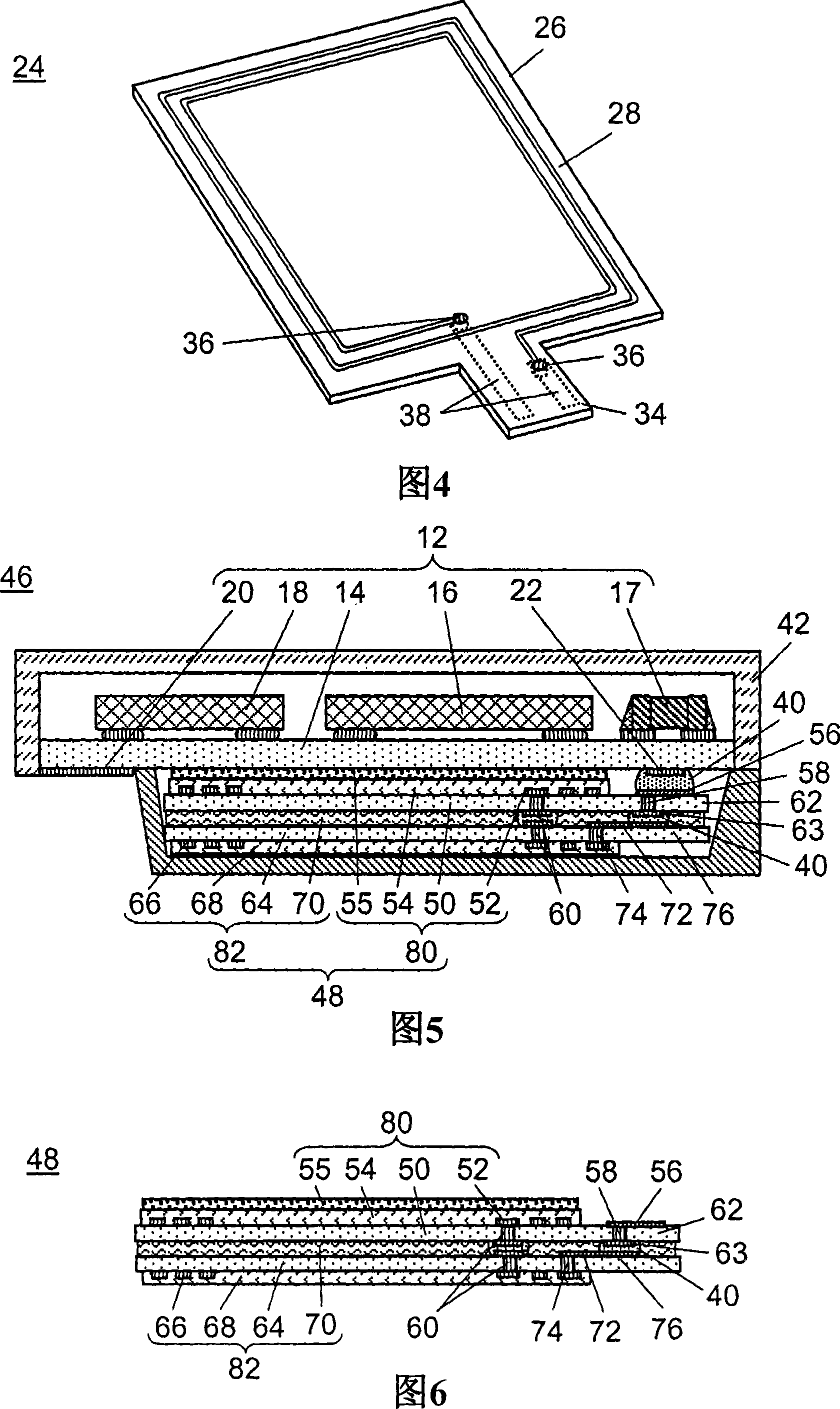
[0103] FIG. 5 is a cross-sectional view of an SD memory card 46 according to a second embodiment of the present invention. As shown in FIG. 5 , the SD memory card 46 of this embodiment is characterized in that the configuration of the antenna module 48 is different from that of the SD memory card 10 of the first embodiment.
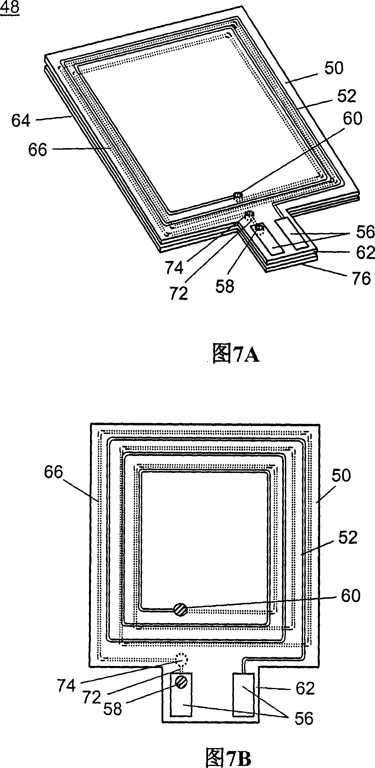
[0104] That is, in the SD memory card 46 of this embodiment, the antenna module 48 has a structure in which the first antenna module 80 and the second antenna module 82 are laminated. FIG. 6 is a schematic cross-sectional view showing the configuration of the antenna module 48 of the present embodiment. 7A is a schematic perspective view of the antenna module 48, and FIG. 7B is a schematic plan view of the antenna module viewed from the first antenna module 80 side. In addition, in FIGS. 7A and 7B , the insulating protection layer 54 and the magnetic layer 55 formed on the first antenna 52 of the first antenna module 80 are omitted for ease of understand...
no. 3 Embodiment approach
[0132] FIG. 10 is a cross-sectional view illustrating the structure of an SD memory card 180 according to a third embodiment of the present invention. The SD memory card 180 of this embodiment is characterized in that the first antenna module 202 and the second antenna module 204 constituting the antenna module 206 are respectively connected to the antenna connection terminal 2201 of the wiring board 1401 .
[0133] A semiconductor memory element 16 and a control semiconductor element 18 are mounted on one surface of a wiring board 1401 of the mounted module 1201, and a connection terminal 20 is formed at one end of the other surface. Furthermore, an antenna connection terminal 2201 for connecting to the respective antenna terminal electrodes 185 and 198 of the first antenna module 202 and the second antenna module 204 is provided at the other end portion of the other surface.
[0134] FIG. 11 is a schematic plan view of the antenna module 206 viewed from the first antenna mod...
PUM
 Abstract
Description
Claims
Application Information
 - Generate Ideas
- Intellectual Property
- Life Sciences
- Materials
- Tech Scout
- Unparalleled Data Quality
- Higher Quality Content
- 60% Fewer Hallucinations
Browse by: Latest US Patents, China's latest patents, Technical Efficacy Thesaurus, Application Domain, Technology Topic, Popular Technical Reports.
© 2025 PatSnap. All rights reserved.Legal|Privacy policy|Modern Slavery Act Transparency Statement|Sitemap|About US| Contact US: help@patsnap.com


