Printed circuit board and method of manufacturing the same

A technology of printed circuit boards and circuit patterns, which is applied in the direction of printed circuit manufacturing, printed circuits, printed circuits, etc., and can solve the problems of reduced precision, increased processing time and processing costs, etc.

Inactive Publication Date: 2008-01-02
SAMSUNG ELECTRO MECHANICS CO LTD
View PDF2 Cites 11 Cited by
  • Summary
  • Abstract
  • Description
  • Claims
  • Application Information

AI Technical Summary

Problems solved by technology

[0007] However, when a chip is mounted in a printed circuit board using these techniques, since holes must be additionally formed in an insulating material and then interconnections are formed through a plating process for interlayer connection, there is a problem of increasing processing time and processing cost. question
[0008] In addition, these conventional methods of embedding chips in a printed circuit board have a problem that when parts having thicknesses different from each other are buried in the printed circuit board, the precision of the part connected to each part is lowered

Method used


Image

  • Printed circuit board and method of manufacturing the same
  • Printed circuit board and method of manufacturing the same
  • Printed circuit board and method of manufacturing the same

Examples


Embodiment Construction

[0025] Hereinafter, the preferred embodiments of the present invention will be described in detail with reference to the accompanying drawings.

[0026] Reference is now made to the drawings, in which the same reference numerals are used throughout the different drawings to indicate the same or similar parts.

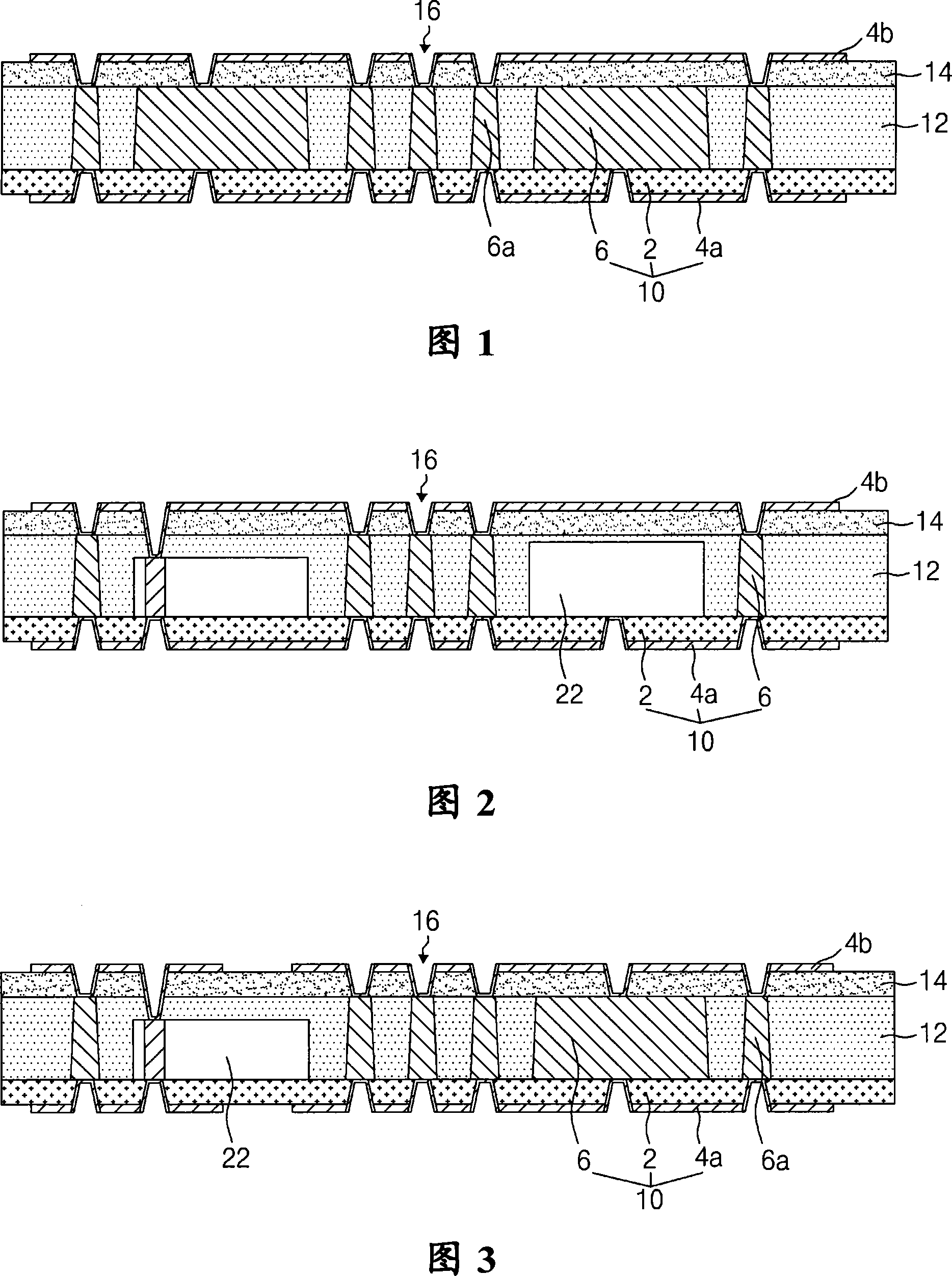
[0027] Fig. 1 is a cross-sectional view showing a printed circuit board according to a first embodiment of the present invention.

[0028] 1, the printed circuit board according to the first embodiment of the present invention includes: a substrate 10 including a first insulating layer 2, a first circuit pattern 4a layered on a lower portion of the first insulating layer 2, and forming The plurality of interlayer connectors 6a and the heat radiation layer 6 on the upper part of the first insulating layer 2; the second insulating layer 12 is layered on the first insulating layer 2; the third insulating layer 14 is layered on the second insulating layer On the upper part of t...


PUM


Abstract

Disclosed herein are a printed circuit board and a method of manufacturing the same, which can achieve reliable heat resistance because heat radiation characteristics are improved, and processing costs of which are reduced because processing times are shortened.

Description

[0001] Cross reference to related applications [0002] This application claims the rights and interests of Korean Patent Application No. 10-2006-0060803 entitled "Printed Circuit Board and Fabricating Method of the Same" filed on June 30, 2006, and its disclosure The whole is incorporated here as a reference. Technical field [0003] The present invention relates to a printed circuit board and a manufacturing method thereof, and more specifically, to a printed circuit board and a manufacturing method thereof that can ensure reliability by improving heat radiation performance and reduce processing costs by shortening processing time. Background technique [0004] As portable electronic products tend to be miniaturized, the space for mounting semiconductors therein has gradually decreased, and electronic products have become more multifunctional. Therefore, the semiconductor package must be light, thin, short, and small to increase the semiconductor mounting efficiency per unit vol...

Claims


Application Information

Patent Timeline
Patent Type & Authority Applications(China)
IPC IPC(8): H05K1/00H05K1/11H05K3/46H05K3/42
CPCH01L2224/04105H01L2924/01002H05K3/4652H05K3/4647H05K1/0204H05K2201/09509H05K1/0206H01L2924/01015H01L2224/2518H05K3/4038H05K3/06H01L2924/3025H01L2924/01006H01L2924/01078H01L23/5389H01L2224/18H01L2924/14H01L24/25H01L2924/01005H01L2224/82039H01L2224/92144H01L24/82H05K2203/0733H05K1/185H01L2924/01029H01L23/3735Y10T29/49155Y10T29/49126H01L2924/01033H05K2201/096H05K3/4602H01L2224/19H05K1/11
Inventor 曹硕铉闵炳烈柳济光徐海男金昞文赵志弘曹汉瑞
Owner SAMSUNG ELECTRO MECHANICS CO LTD
Why Eureka
Try Eureka