
Long wavelength laser transmitted perpendicular to surface of cavity by using integrated pumping light source

A technology of vertical cavity surface emission and fabrication method, which is applied in the field of long wavelength vertical cavity surface emitting lasers, and can solve the problems of device cost, increased packaging difficulty, difficult temperature characteristics, and difficulty in heat dissipation.

Inactive Publication Date: 2007-12-26
INST OF SEMICONDUCTORS - CHINESE ACAD OF SCI
View PDF0 Cites 13 Cited by
  • Summary
  • Abstract
  • Description
  • Claims
  • Application Information

AI Technical Summary

Problems solved by technology

[0009] 2) The Auger absorption and valence band absorption of InGaAsP / InP materials are relatively large
[0010] 3) InGaAsP and InP systems have very small potential barriers on the conduction band, especially when the carrier concentration is high, it is difficult to have better temperature characteristics
[0011] 4) The thermal conductivity of InGaAsP material is relatively low, and it is difficult to dissipate heat, which leads to low laser power
[0012] 5) InGaAsP / InP materials currently do not have a good current confinement method
These shortcomings of InGaAsP / InP materials make the single-mode output power of long-wavelength surface-emitting lasers very low, which cannot meet the requirements of optical communication systems
[0013] In order to overcome the problem of low single-mode output power of vertical cavity surface emitting lasers, the researchers used light instead of electricity to pump long wavelength surface emitting lasers
The heat generation of optically pumped vertical surface emitting lasers is significantly smaller than that of electrically pumped vertical cavity surface emitting lasers, so higher single-mode output power can be obtained, but the introduction of an external pump light source greatly increases the cost of the device and the difficulty of packaging. Difficult to scale up

Method used


Image

  • Long wavelength laser transmitted perpendicular to surface of cavity by using integrated pumping light source
  • Long wavelength laser transmitted perpendicular to surface of cavity by using integrated pumping light source

Examples


Embodiment

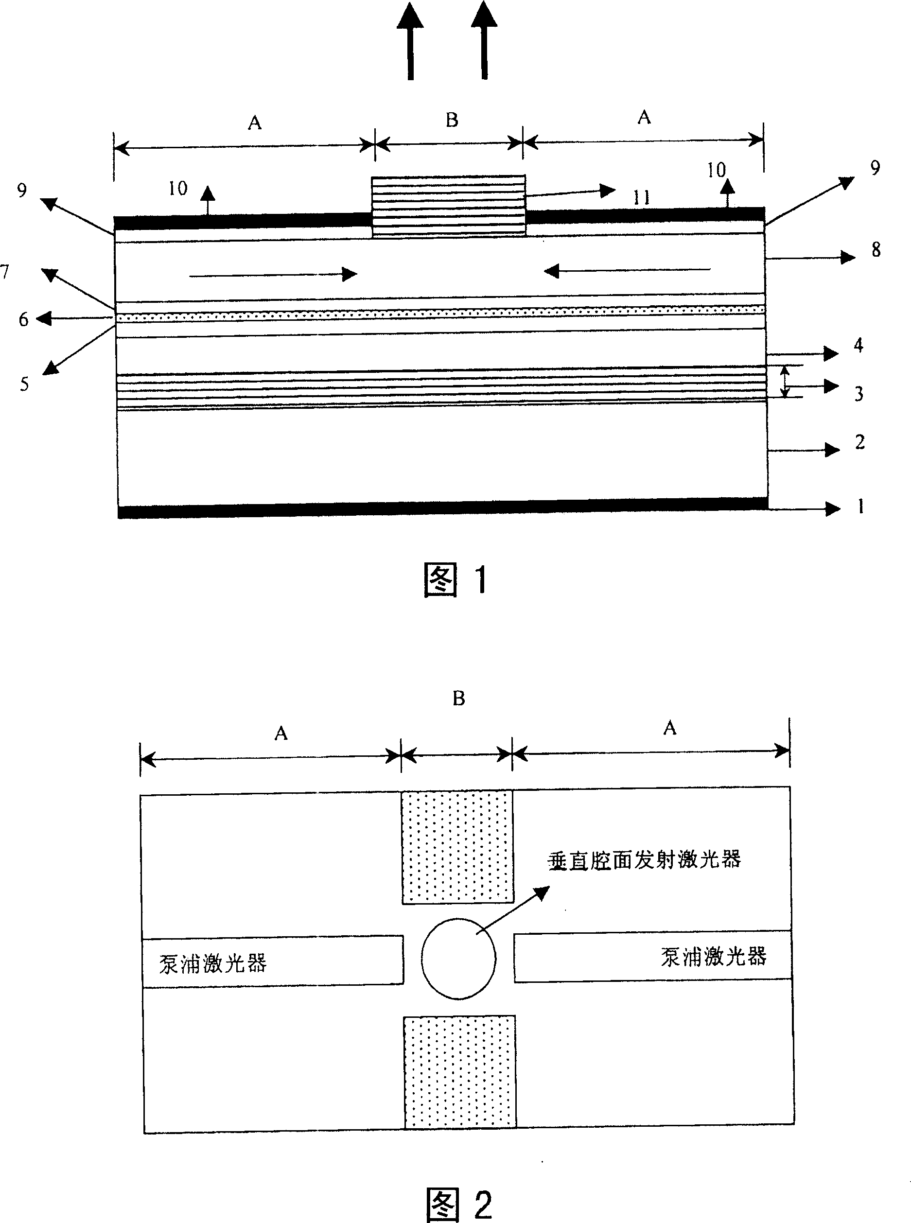
[0079] Please refer to Fig. 1 and Fig. 2, the long-wavelength vertical cavity surface emitting laser structure of the integrated pump light source of the present invention includes: a lower electrode 1, a substrate 2, a lower Bragg reflector (DBR) 3, a lower confinement layer 4, Lower waveguide layer 5 , active region 6 , upper waveguide layer 7 , upper confinement layer 8 , ohmic contact layer 9 , upper electrode 10 and upper Bragg reflector (DBR) 11 .

[0080] The lower electrode 1 is Au-Ge-Ni;

[0081] Substrate 2 is an n-type InP substrate;

[0082] The lower Bragg reflector (DBR) 3 is 40 pairs of AlGaInAs / InP lattice-matched with InP, doped into n-type. It has a larger refractive index difference, a lower conduction band potential difference and a higher thermal conductivity;

[0083] The lower confinement layer 4 is n-type InP;

[0084] The lower waveguide layer 5 is InGaAsP with a bandgap wavelength of 1.2 μm, without doping;

[0085] The active region 6 is divided ...


PUM


Abstract

The laser device includes a substrate; a Bragg reflector prepared on the substrate; a low limiting layer prepared on the Bragg reflector; a low waveguide layer prepared on the low limiting layer, and band gap wavelength of the low waveguide layer being as indium-gallium-arsenic-phosphor material in 1.2 micron; an active region prepared on the low waveguide layer; an up waveguide layer prepared on the active region, and band gap wavelength of the up waveguide layer being as indium-gallium-arsenic-phosphor material in 1.2 micron; an up limiting layer prepared on the up waveguide layer; an up Bragg reflector prepared at middle on the up limiting layer; being prepared on the up limiting layer, an ohmic contact layer is located at two sides of the up Bragg reflector; being prepared on the ohmic contact layer, an up electrode is located at two sides of the up Bragg reflector; a low electrode prepared underside of the substrate.

Description

technical field [0001] The invention is a vertical cavity surface emitting laser (Vertical Cavity Surface Emitting Laser, VCSEL), especially a long wavelength vertical cavity surface emitting laser integrated with a pumping light source (edge ​​emitting laser). Background technique [0002] Vertical cavity surface emitting laser (Vertical Cavity Surface Emitting Laser, VCSEL) is a promising semiconductor laser, it has many advantages: [0003] 1) It can be made into a densely arranged two-dimensional laser array. [0004] 2) A thin circular beam can be emitted from the direction perpendicular to the substrate, and the coupling efficiency with the optical fiber is high. [0005] 3) It can be tested before the chip is understood, which greatly reduces the cost. [0006] 4) Good dynamic single-mode performance and wide modulation bandwidth. Because vertical cavity surface emitting lasers have so many features superior to traditional edge emitting lasers, they quickly became ...

Claims


Application Information

Patent Timeline
Patent Type & Authority Applications(China)
IPC IPC(8): H01S5/183H01S5/20H01S5/187H01S5/04H01S5/343
Inventor 吴旭明王小东谭满清
Owner INST OF SEMICONDUCTORS - CHINESE ACAD OF SCI
Learn More