
Manufacturing method of low cost DFB laser

A DFB laser and manufacturing method technology, which is applied to lasers, laser parts, semiconductor lasers, etc., can solve the problems of high mass production cost, inability to manufacture multi-wavelength DFB laser arrays, and inability to manufacture phase-shift gratings, etc. The effect of yield

Inactive Publication Date: 2007-07-18
GUANGXUN SCI & TECH WUHAN +1
View PDF0 Cites 35 Cited by
  • Summary
  • Abstract
  • Description
  • Claims
  • Application Information

AI Technical Summary

Problems solved by technology

[0006] The purpose of the present invention is to address the shortcomings of using double-beam interference method or electron beam exposure method in the production of existing semiconductor laser gratings, and propose a low-cost DFB laser production method based on nanoimprint technology, which effectively overcomes the usual The double-beam interferometry cannot produce phase-shifting gratings, cannot simultaneously produce multi-wavelength DFB lasers for DWDM on the same epitaxial wafer, and cannot produce multi-wavelength DFB laser arrays or DFB-EA arrays on the same chip; at the same time, it also overcomes the shortcomings of electron beam Disadvantages of high cost of mass production by exposure method

Method used


Image

  • Manufacturing method of low cost DFB laser
  • Manufacturing method of low cost DFB laser
  • Manufacturing method of low cost DFB laser

Examples


Embodiment Construction

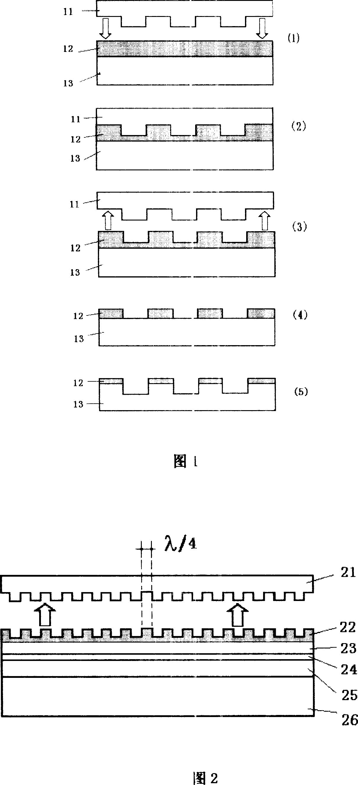
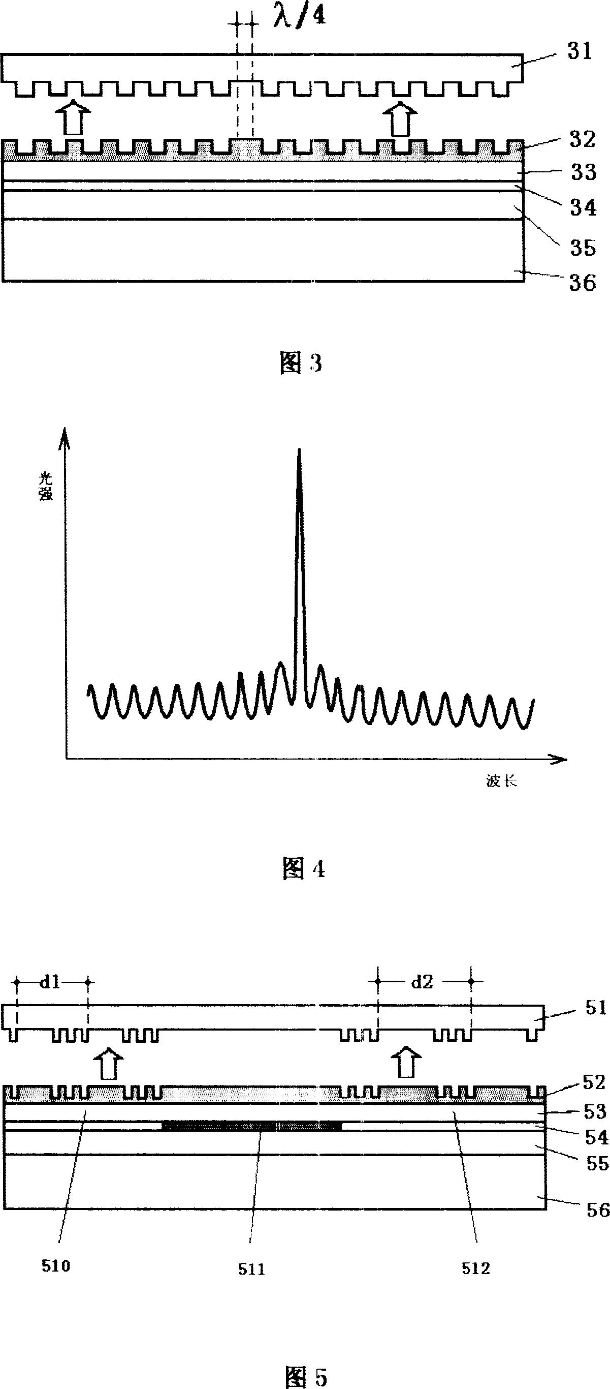
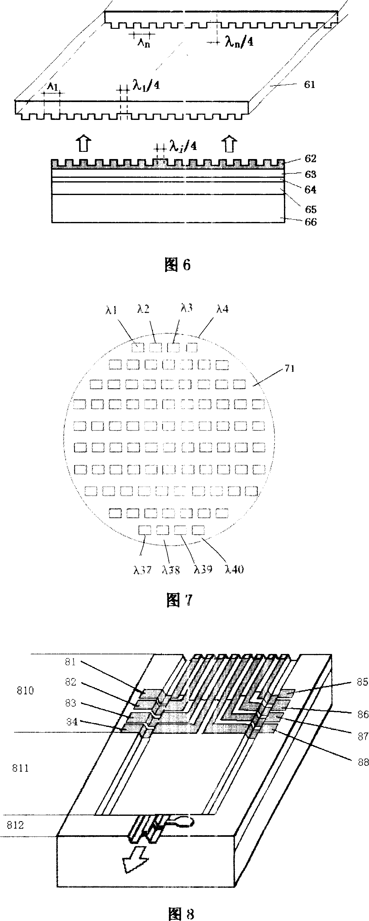
[0026] The invention makes active optoelectronic devices such as DFB gratings of semiconductor lasers by adopting nano imprinting technology. The semiconductor laser grows the lower cladding layer, the lower waveguide layer, the active layer, the upper waveguide layer, the upper cladding layer and the electrode contact layer sequentially on the InP substrate. There are metal electrodes on the substrate and the electrode contact layer respectively, and the upper waveguide layer Or there is a distributed feedback Bragg grating (DFB) structure on the lower waveguide layer. The method for manufacturing DFB gratings by adopting nanoimprinting technology has the characteristics of low manufacturing cost, high production efficiency and high grating resolution.

[0027] The scheme of the invention is suitable for making DFB gratings by adopting thermal embossing technology; it is suitable for making DFB gratings by adopting ultraviolet hardening embossing technology; it is suitable fo...


PUM


Abstract

The invention relates to a method for manufacturing a low-cost DFB laser. The semiconductor laser is composed of a lower coating layer, a lower waveguide layer, a active layer, a upper waveguide layer, a upper coating layer and a electrode contact layer, the above items all grow on the InP substrate in a proper sequence, and there are metal electrodes on the substrate and the electrode contact layer, and there is a grating structure on the upper waveguide layer or the lower waveguide layer. Its characters show as follow: the described DFB grating structure is manufactured by via nano-imprint technology. It can be an arbitrary phase shift structure of the grating or arbitrary sampling structure of the grating.

Description

technical field [0001] The invention relates to a method for manufacturing a DFB grating of an active optoelectronic device, belonging to the technical field of active optical devices. Background technique [0002] Semiconductor lasers are the most important light sources in optical communication systems. With the rapid development of optical fiber communication in the direction of long distance and large capacity, semiconductor lasers are increasingly required to have high-speed, narrow linewidth and dynamic single longitudinal mode working characteristics. It is generally believed that the laser with distributed feedback Bragg grating (DFB) is the most ideal light source to meet the requirements of long-distance and large-capacity optical fiber communication systems. [0003] The spectrum of the F-P laser with common structure is multi-longitudinal mode, and there is spectral broadening under high-speed modulation, which reduces the transmission bandwidth of the fiber, th...

Claims


Application Information

Patent Timeline
Patent Type & Authority Applications(China)
IPC IPC(8): H01S5/12H01S5/125
Inventor 刘文王定理周宁孙飞黄德修
Owner GUANGXUN SCI & TECH WUHAN
Learn More