
Silicon base efficient multi-node solar battery and its making method

A multi-junction solar cell, high-efficiency technology, applied in the direction of circuits, photovoltaic power generation, electrical components, etc., can solve the problems of low conversion efficiency, high cost, and difficult production of single-junction solar cells, and achieve the solution of lattice mismatch and electrical components. The effect of missing allocation problem, saving cost and simplifying production process

Inactive Publication Date: 2009-12-23
SUZHOU INST OF NANO TECH & NANO BIONICS CHINESE ACEDEMY OF SCI
View PDF3 Cites 0 Cited by
  • Summary
  • Abstract
  • Description
  • Claims
  • Application Information

AI Technical Summary

Problems solved by technology

[0005] The purpose of the present invention is to develop a silicon-based high-efficiency multi-junction solar cell to solve the problem of low conversion efficiency of single-junction solar cells in the prior art, and the high cost and difficulty of making multi-junction solar cells using Ge. question

Method used


Image

  • Silicon base efficient multi-node solar battery and its making method

Examples


Embodiment 1

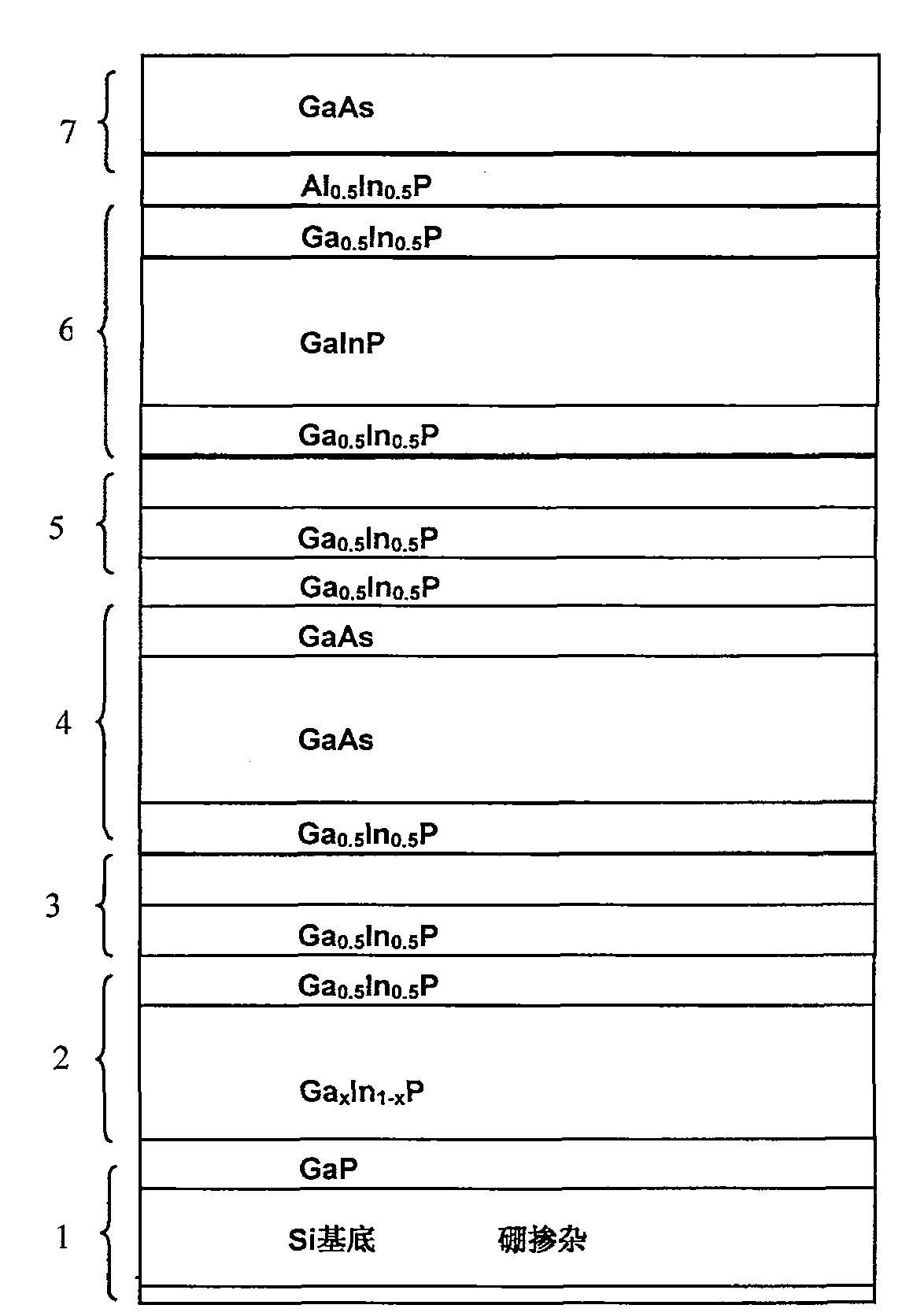
[0030] Embodiment one: see attached figure 1 As shown, a method for preparing a silicon-based high-efficiency multi-junction solar cell comprises the following steps:

[0031] 1. Use a p-type doped single crystal silicon substrate with a thickness of about 100 to 150 microns and a concentration of 5×10 15 cm -3 to 10 17 cm -3 Between, as the base region of Si solar cells, the surface of the substrate can first diffuse 1×10 -19 cm -3 The above boron, highly doped P-type silicon layer acts as the back field of the solar cell, preventing the photogenerated electrons in the base region from being recombined by the back electrode;

[0032] 2. Enter MOCVD growth, first grow a layer of n-type highly doped GaP layer about 0.2 microns thick, the lattice constant of GaP is close to that of Si substrate, because the high temperature in the growth process makes both Ga and P atoms have Diffusion to Si, and P is relatively easy to diffuse, automatically forming a highly doped n-type ...


PUM


Abstract

The present invention discloses a silicon-based high-efficient multiple solar cell which comprises a top layer sub-cell, a middle sub-cell and a base sub-cell, each sub-cell is connected through the channels to form a series-connected structure, and the invention has the following characters: the base sub-cell is PN cells of the Si, the middle sub-cell is PN cells of GaAs, the top sub-cell is PN cells of GaInP, each sub-cell and the connection structure therebetween are obtained by directly growing on the silicon monocrystal substrate. The invention can sufficiently utilize the mature production technique of the existing silicon solar cell, settle the problem of unmatching of the Si and GaAs crystal lattice, the conversion efficiency can be increased to above 28and the existing theoretic limit of the Si solar cell can be exceeded.

Description

technical field [0001] The present invention relates to a device for converting sunlight radiation energy into electrical energy, and a method for manufacturing the device, in particular to a silicon-based high-efficiency multi-junction solar cell, especially Si, GaAs(P), InGaP and A stacked multi-junction solar cell with a pn junction as a photoelectric conversion layer and a preparation method thereof. Background technique [0002] Solar cells are an important strategic way to solve the world's energy problems. At present, the mass-produced solar cells on the market are monocrystalline and polycrystalline silicon solar cells, and their average efficiency is around 15%, which means that solar cells can only convert 15% of the incident solar energy into usable electrical energy, and the remaining 85% are converted. for thermal energy. The generation of heat energy not only causes a huge waste of energy, but also brings about the technical problem of heat dissipation, which...

Claims


Application Information

Patent Timeline
Patent Type & Authority Patents(China)
IPC IPC(8): H01L31/068H01L31/18H01L31/0687
CPCY02E10/50Y02E10/544Y02P70/50
Inventor 张耀辉董建荣余庭黄伍桥
Owner SUZHOU INST OF NANO TECH & NANO BIONICS CHINESE ACEDEMY OF SCI
Learn More