Preparation of metal silicon nitride films via cyclic deposition
A deposition method and nitride technology, applied in metal material coating process, household appliances, gaseous chemical plating, etc., to achieve the effect of increasing wafer yield
- Summary
- Abstract
- Description
- Claims
- Application Information
AI Technical Summary
Problems solved by technology
Method used
Image

Examples
Embodiment 1
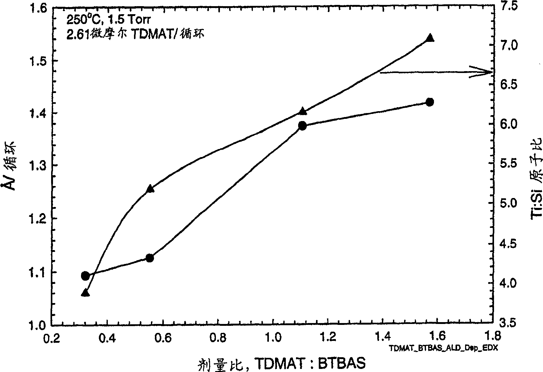
[0077] TiSiN Thin Films Deposited by TDMAT and BTBAS at 200℃
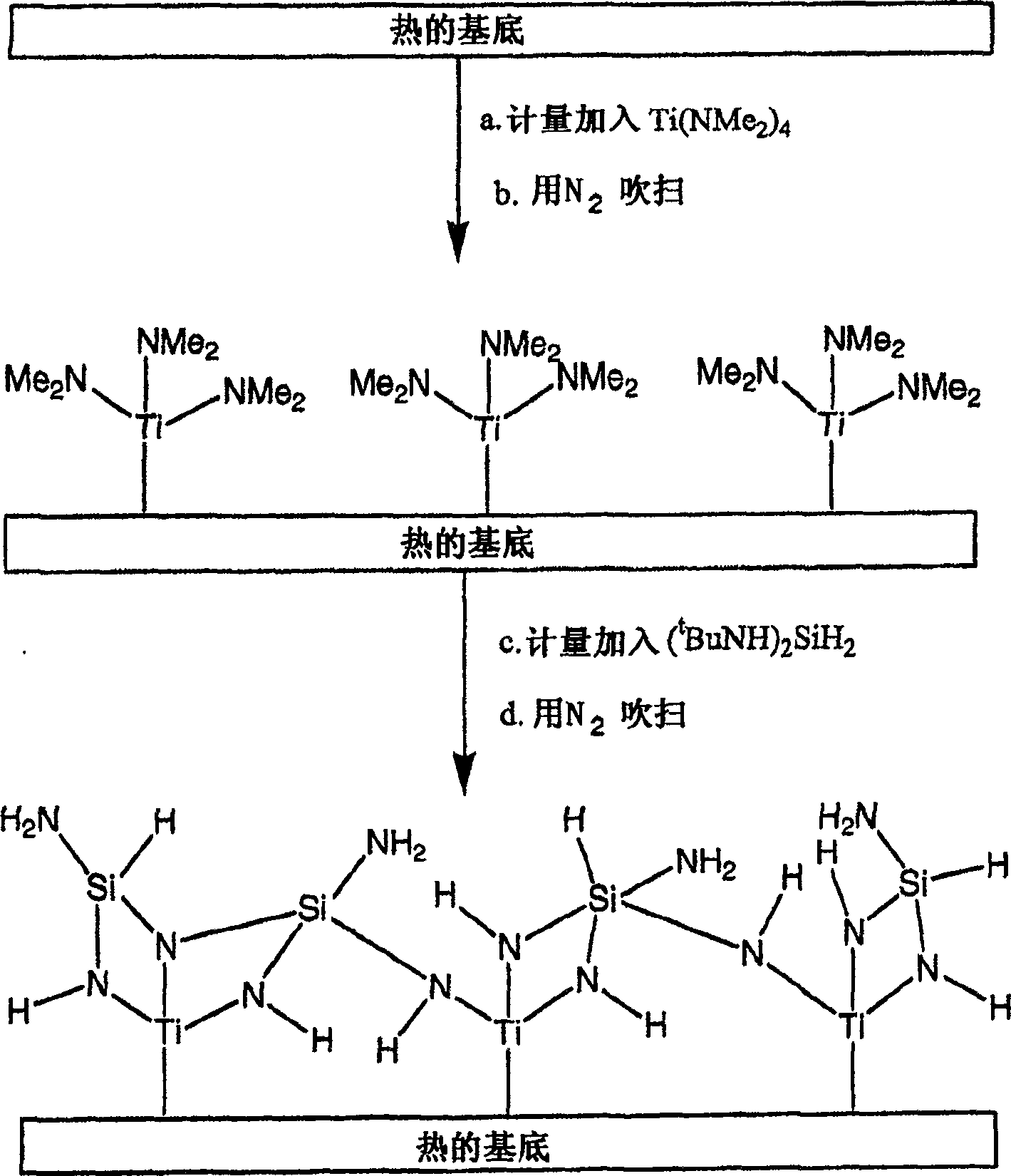
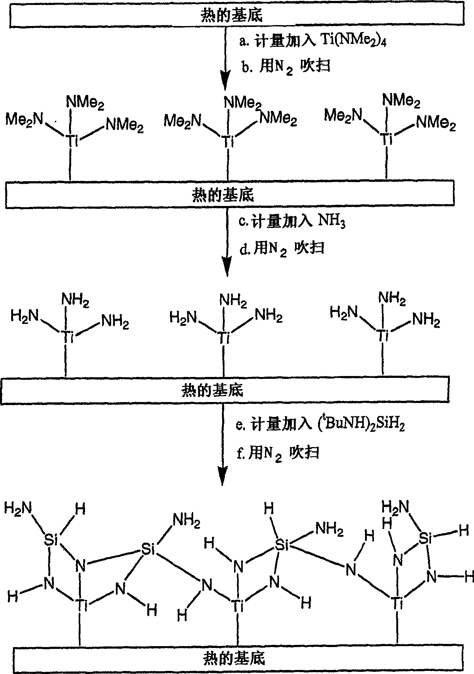
[0078] The silicon wafer was placed in the deposition chamber and maintained at a temperature of 200°C and a pressure of 200 Pa (1.5 Torr). 2.6 micromoles of the titanium-containing compound, tetrakis(dimethylamino)titanium (TDMAT), was introduced into the deposition chamber along with 100 sccm of nitrogen gas in 10 second pulses. After titanium amide deposition, use 2000 sccm N 2 Unreacted titanium amides and by-products were purged for 7.5 seconds. Then, 4.73 micromoles of the silicon-containing compound, bis(tert-butylamino)silane (BTBAS), were introduced together with 100 sccm of nitrogen over 80 seconds. Unreacted BTBAS and by-products were purged with 2000 seem nitrogen for 40 seconds.
[0079] The above cycle was repeated 200 times (4 steps), resulting in a 45 angstrom thick layer. The deposition rate per cycle is 0.22 angstroms, which is much lower than that of the general ALD method, indicating that th...
Embodiment 2
[0081] Formation of TiSiN thin films by TDMAT and BTBAS using ALD method at 250 °C
[0082] The operation of Example 1 was followed, except that the wafer was placed at a temperature of 250° C. and a pressure of 200 Pa (1.5 Torr). 2.6 micromoles of a titanium-containing compound, tetrakis(dimethylamino)titanium (TD MAT), was introduced into the deposition chamber for 10 seconds along with 100 sccm of nitrogen. This is followed by a nitrogen purge of 2000 sccm for 7.5 seconds. Then, 4.73 micromoles of a silicon-containing compound, bis(tert-butylamino)silane (BTBAS), was introduced together with 100 sccm of nitrogen for 80 seconds. This is followed by a nitrogen purge of 2000 sccm for 40 seconds. The above cycle was repeated 100 times (4 steps), resulting in a 144 angstrom thick layer.
[0083] The deposition rate per cycle was 1.44 Angstroms, which falls within the range of typical ALD methods, indicating that this temperature is sufficient to saturate the monolayer surface...
Embodiment 3
[0086] Formation of TiSiN thin films by TDMAT and BTBAS using cyclic CVD method
[0087] The operation of Example 1 was followed, except that the silicon wafer was placed at a temperature of 300° C. and a pressure of 200 Pa (1.5 Torr). 2.6 micromoles of tetrakis(dimethylamino)titanium (TDMAT) was introduced into the deposition chamber for 10 seconds as the titanium-containing compound along with 100 sccm of nitrogen gas. This is followed by a nitrogen purge of 2000 sccm for 7.5 seconds. Then, 4.73 micromoles of a silicon-containing compound, bis(tert-butylamino)silane (BTBAS), was introduced together with 100 sccm of nitrogen for 80 seconds. This is followed by a nitrogen purge of 2000 sccm for 40 seconds. The above cycle was repeated 100 times (4 steps), resulting in a 629 Angstrom thick layer. The deposition rate per cycle was 6.29 Angstroms, indicating that the temperature was too high to limit the deposition of a single layer per cycle. In contrast to Examples 1 and 2,...
PUM
 Abstract
Description
Claims
Application Information
 - R&D
- Intellectual Property
- Life Sciences
- Materials
- Tech Scout
- Unparalleled Data Quality
- Higher Quality Content
- 60% Fewer Hallucinations
Browse by: Latest US Patents, China's latest patents, Technical Efficacy Thesaurus, Application Domain, Technology Topic, Popular Technical Reports.
© 2025 PatSnap. All rights reserved.Legal|Privacy policy|Modern Slavery Act Transparency Statement|Sitemap|About US| Contact US: help@patsnap.com