
A canal step channel unit transistor and its manufacture method

A manufacturing method and technology of transistors, which can be used in semiconductor/solid-state device manufacturing, electrical components, electrical solid-state devices, etc., and can solve problems such as leakage

Inactive Publication Date: 2009-06-24
PROMOS TECH INC
View PDF6 Cites 0 Cited by
  • Summary
  • Abstract
  • Description
  • Claims
  • Application Information

AI Technical Summary

Problems solved by technology

[0003] Among them, in view of the short channel effect (Short Channel Effect) caused by the reduction of the current channel length due to the reduction of the size of the semiconductor element, some people use the Recess Channel Array Transistor or the Step Transistor Array This method increases the length of the current channel, but when manufacturing a device structure with deep trench capacitance, the disadvantage of this method is that it will cause the current to punch through due to the diffusion of the Buried Strap electrode. resulting in leakage
[0004] Lim, S.-H. and others have done related research on the growth rate and temperature of isotropic and anisotropic selective epitaxial growth methods (see Isotropic / anisotropic selective epitaxial growth of Si and SiGe on LOCOS patterned Si(100 )substrate by cold walltype UHV-CVD, from Microprocesses and Nanotechnology conference, 2002.Digest of Papers.Microprocesses and Nanotechnology 2002.2002International 6-8 Nov.2002 Page(s):74-75), found that when the operating temperature is 600℃ At 650°C, anisotropic selective epitaxial growth is quite close to unidirectional epitaxial growth; at 650°C, complete selective unidirectional epitaxial growth can be achieved, but no one has used this method in the channel process of transistors

Method used


Image

  • A canal step channel unit transistor and its manufacture method
  • A canal step channel unit transistor and its manufacture method
  • A canal step channel unit transistor and its manufacture method

Examples


Embodiment Construction

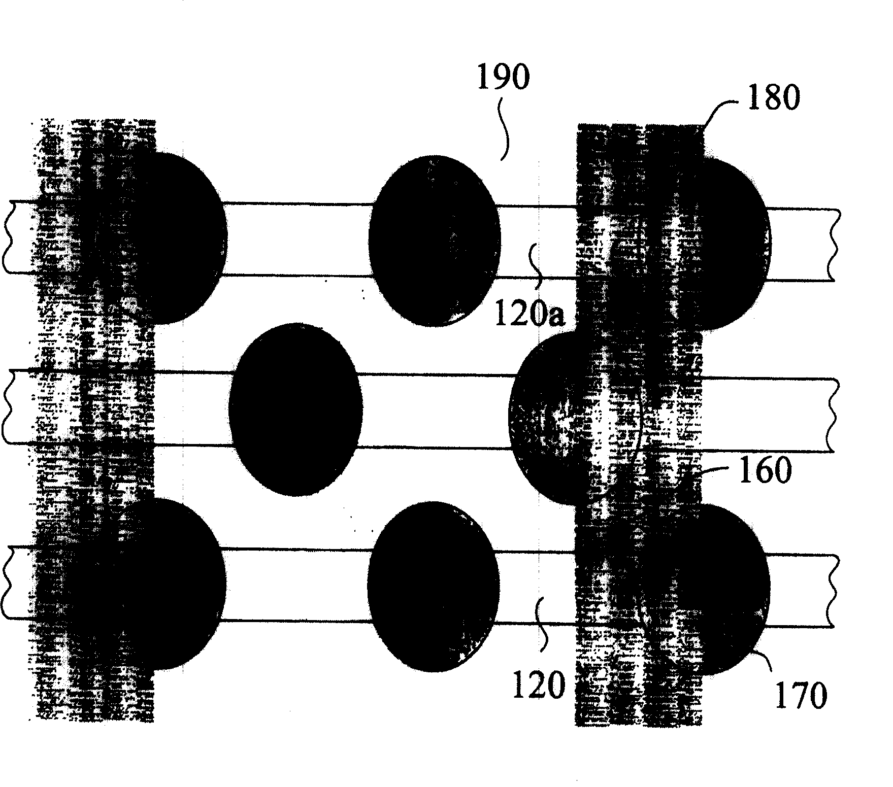
[0057] figure 1 A trench step channel unit transistor applying the technology of the present invention is shown, and the figure shows a schematic diagram of the relative positions of the components of the present invention. The channel of the trench stepped channel transistor of the present invention mainly includes an anisotropic stepped silicon layer 110 and an active element region 120 in the substrate 100, wherein the substrate 100 has a trench capacitor structure, and the capacitor structure includes a deep trench structure 170, The first electrode 260, the insulating layer 270, the second electrode 280, the buried conductor layer 290, and the like.

[0058] Secondly, in terms of position setting, the anisotropic step silicon layer 110 is located above the active element region 120, the deep trench structure 170 is located in the substrate 100, and the first electrode 260 is located in the substrate 100 and surrounds the lower edge of the deep trench structure 170 , the ...


PUM


Abstract

A trench step channel (Trench Step Channel, TSC for short) unit transistor and its manufacturing method are used to increase the channel length of the transistor, and the transistor includes a selectively grown step silicon layer. Wherein the step silicon crystal layer is located above the active element area of ​​the transistor.

Description

technical field [0001] The present invention relates to a trench step channel (Trench Step Channel; TSC for short) unit transistor and a manufacturing method thereof, in particular to a trench step channel (TSC) unit transistor with a selectively grown step silicon layer and its method of manufacture. Background technique [0002] The industrial revolution in the 19th century mainly saved manpower with machines, and in the 20th century, computers further solved the even greater demand for manpower. In 1947, W. Schockley and others invented the transistor to replace the vacuum tube amplifier, which opened the development of the microelectronics industry. At the end of the 20th century, the development of miniaturization of electronic technology greatly reduced the size of electronic equipment. With the development of semiconductor As the integration level of circuits increases, the size of semiconductor components must also be reduced accordingly. Today, electronic material...

Claims


Application Information

Patent Timeline
Patent Type & Authority Patents(China)
IPC IPC(8): H01L21/82H01L21/336H01L27/02H01L29/78
Inventor 钟朝喜
Owner PROMOS TECH INC
Learn More