Making method of the pixel structure and pixel structure

A manufacturing method and technology of pixel structure, applied in semiconductor/solid-state device manufacturing, optics, instruments, etc., can solve the problems of high total production cost, low production qualification rate, long production time, etc., to reduce photocurrent and improve production. Qualification rate, effect of improving characteristics

Active Publication Date: 2009-05-27
AU OPTRONICS CORP
View PDF7 Cites 0 Cited by
  • Summary
  • Abstract
  • Description
  • Claims
  • Application Information

AI Technical Summary

Problems solved by technology

When the manufacturing steps are more complicated, the pixel structure 90 has a higher chance of producing defects, and the production pass rate is also lower.
In addition, the production of the pixel structure 90 in the prior art requires more production steps and takes a longer production time. Whether it is the fixed cost of purchasing machine equipment or the cost of materials for production and utilization, the total production cost will be reduced. Becomes high

Method used


Image

  • Making method of the pixel structure and pixel structure
  • Making method of the pixel structure and pixel structure
  • Making method of the pixel structure and pixel structure

Examples


no. 1 example

[0072] Figure 2A ~ Figure 2I It is the manufacturing method of the pixel structure of the first embodiment of the present invention.

[0073] Please refer to Figure 2A , first provide a substrate 210 having a pixel region P. Next, a first metal layer 220, a gate insulating layer 230, and a semiconductor layer 240 are sequentially formed on the substrate 210, wherein the material of the semiconductor layer 240 is, for example, amorphous silicon or polysilicon, and the method of forming the first metal layer 220 is, for example, sputtering. (sputtering) or evaporation (evaporation). The material of the gate insulating layer 230 is, for example, silicon oxide or silicon nitride or a laminate thereof, and the method of forming the gate insulating layer 230 is, for example, chemical vapor deposition (CVD). Then, if Figure 2A As shown, the first metal layer 220, the gate insulating layer 230, and the semiconductor layer 240 are patterned through the first half-tone or gray-to...

no. 2 example

[0087] Figure 3A ~ Figure 3I It is the manufacturing method of the pixel structure of the second embodiment. The fabrication method of the pixel structure 300 of this embodiment is similar to that of the first embodiment. In this embodiment, the formation of the transistor pattern 250, the lower capacitor pattern 260 and the lower circuit pattern 270 as well as the fabrication of the patterned dielectric layer 280 and the electrode layer 290 way, such as Figure 3A-3D shown, which is consistent with the first embodiment Figure 2A-2D similar and will not be repeated here.

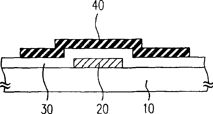
[0088] Also, please refer to Figure 3E In this embodiment, after patterning the dielectric layer 280 and the electrode layer 290, a doped semiconductor layer 240' is formed on the electrode layer 290, and the doped semiconductor layer 240' is connected to the lower circuit pattern 270, the lower capacitor pattern 260 and The source 250a / drain 250b region of the transistor pattern 250 . The doped semi...


PUM


Abstract

The present invention discloses a production method of the pixel structure, including the following steps: firstly providing one substrate with a pixel area; forming a metal layer, a gate insulation layer, and a semiconductor layer on the substrate, and patterning them by a first partly-adjustable or gray-adjustable light shield, to form a transistor pattern, a lower layer capacitance pattern and a lower layer circuit pattern; then, orderly forming a dielectric layer and one electrode layer to cover the said three patterns, then patterning them to expose some lower layer circuits, lower layer capacitances and onesource / drain area of the transistor pattern, and creating a second metal layer on them; then, patterning the second metal layer and the electrode layer by a second partly-adjustable or gray-adjustable light shield to form a upper layer circuit, a source / drain pattern and a upper layer capacitance, and part of the electrode layer constituting a pixel electrode.

Description

technical field [0001] The invention relates to a method for manufacturing a pixel structure, and in particular to a method for manufacturing a pixel structure using fewer photomasks. Background technique [0002] With the advancement of modern video technology, various displays have been widely used on display screens of consumer electronic products such as mobile phones, notebook computers, digital cameras, and personal digital assistants (PDAs). Among these displays, liquid crystal displays (LCDs) and organic electroluminescence displays (OELDs) have become mainstream in the market due to their advantages of light weight, small size, and low power consumption. Regardless of whether it is a liquid crystal display or an organic electroluminescent display, the manufacturing process includes forming an array of pixel structures on a substrate through a semiconductor process. [0003] Figure 1A ~ Figure 1G A cross-sectional flowchart illustrating a manufacturing method of a ...

Claims


Application Information

Patent Timeline
Patent Type & Authority Patents(China)
IPC IPC(8): H01L21/84H01L21/768H01L27/12H01L23/522G02F1/1362
Inventor 陈昱丞
Owner AU OPTRONICS CORP
Why Eureka
Try Eureka