Method for producing active component array base plate
A technology of active components and array substrates, applied in semiconductor/solid-state device manufacturing, electrical components, circuits, etc., can solve the problems of cumbersome manufacturing process and undisclosed issues, and achieve the effect of improving color shift phenomenon
- Summary
- Abstract
- Description
- Claims
- Application Information
AI Technical Summary
Problems solved by technology
Method used
Image

Examples
no. 1 example
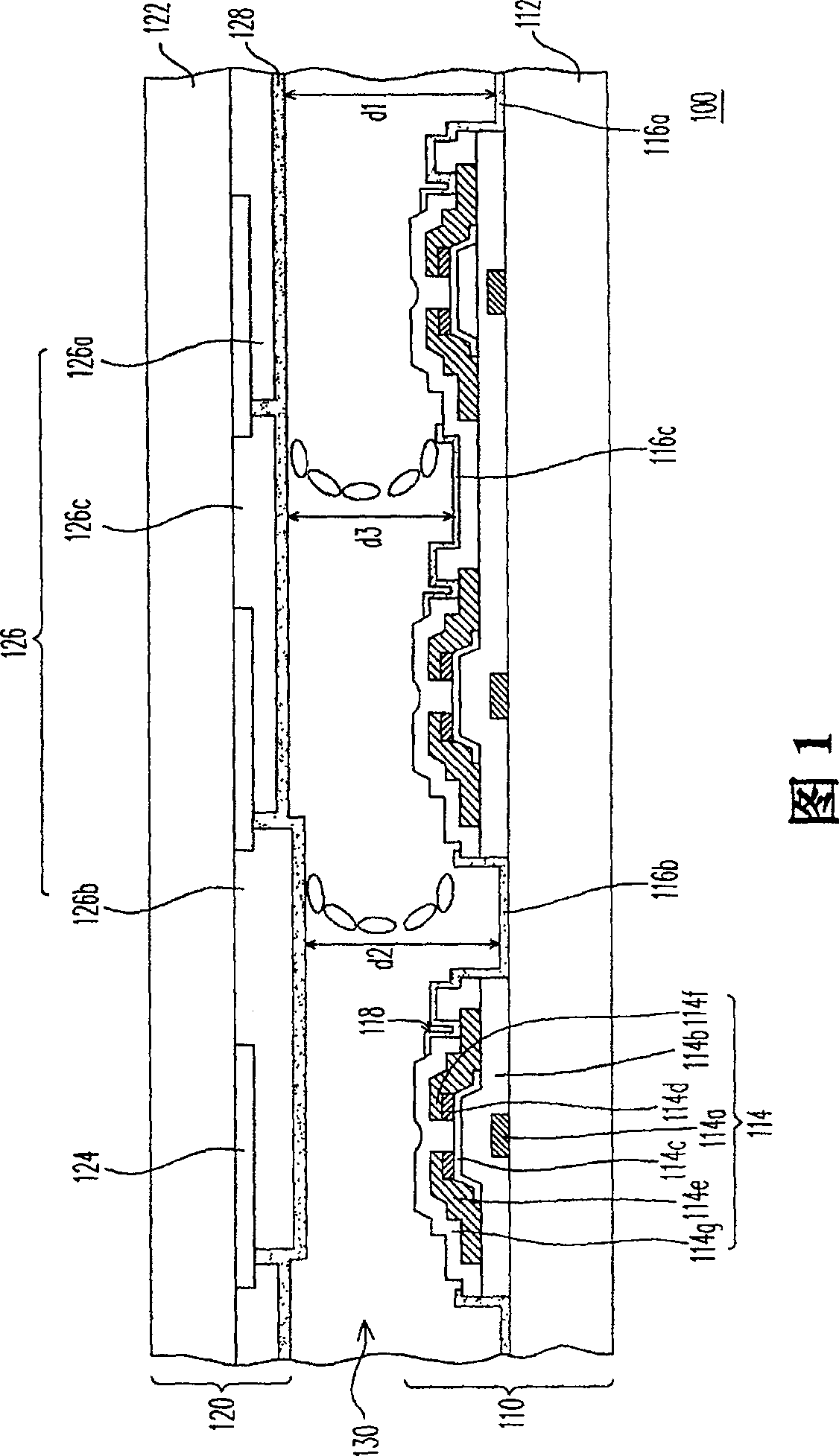
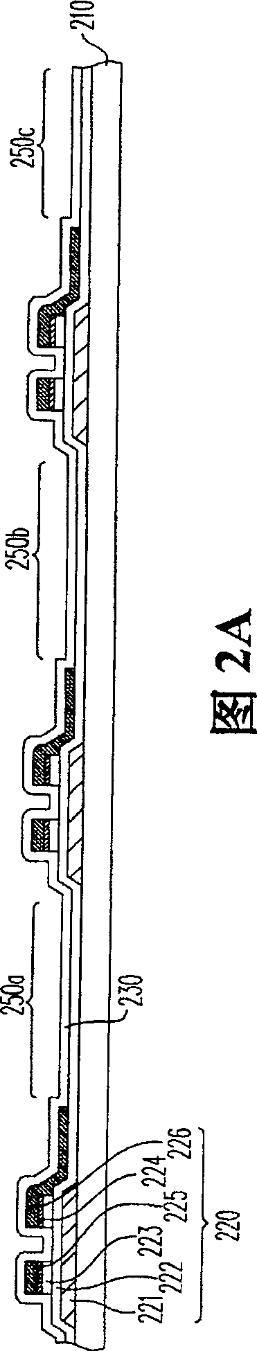
[0081] 2A to 2E are schematic diagrams of the manufacturing process of the active device array substrate according to the first embodiment of the present invention. Referring to FIG. 2A , the manufacturing method of the active device array substrate of this embodiment includes the following steps. Firstly, the substrate 210 is provided, and the scanning wiring (not shown in the figure) and the gate 221 of the active device 220 are formed on the substrate 210 , and the gate 221 is electrically connected to the scanning wiring. Then, a first dielectric layer 222 is formed on the substrate 210 , and the first dielectric layer 222 covers the gate 221 . Next, a channel layer 223 and an ohmic contact layer 224 are formed on the first dielectric layer 222 .
[0082] On the first dielectric layer 222, a data wiring (not shown) and a source 225 and a drain 226 are formed, wherein the data wiring is electrically connected to the source 225, and the source 225 and the drain 226 are arra...
no. 2 example
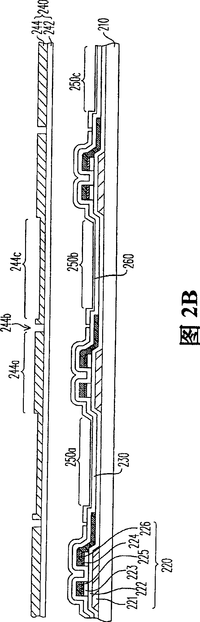
[0093]FIG. 4 is a cross-sectional view of an OCB liquid crystal display panel according to the second embodiment of the present invention. Please refer to FIG. 2B and FIG. 4 , the manufacturing method of the active device array substrate 201 of this embodiment is similar to the manufacturing method of the above-mentioned active device array substrate 200 , the difference is that: due to the partial transparency of the half-tuning photolithography mask 240 The thickness of the patterned photoresist layer 260 on the red pixel region 250a and the green pixel region 250b is also different due to the difference in light transmittance of the light region 244c. Therefore, after forming the contact window 252 and the recessed portion 254, the distances D1, D2 between the pixel electrode 270 on the red pixel region 250a and the green pixel region 250b and the substrate 210 are smaller than the distances D1, D2 between the pixel electrode 270 and the substrate on the blue pixel region 25...
no. 3 example
[0096] FIG. 5 is a cross-sectional view of an OCB liquid crystal display panel according to a third embodiment of the present invention. Please refer to FIG. 5 , the manufacturing method of the active device array substrate 202 of this embodiment is similar to the manufacturing method of the above-mentioned active device array substrates 200 and 201 , the difference is that the pattern formed by the half-tone photolithography mask 240 The photoresist layer 260 (as shown in FIG. 2B ) is used as a mask to completely remove the second dielectric layer 230 and part of the first dielectric layer 222 . Therefore, the distances D1 and D2 between the pixel electrode 270 in the concave portion 254 and the substrate 210 are smaller than the distance D3 between the pixel electrode 270 on the blue pixel region 250c and the substrate 210 . As far as this embodiment is concerned, the relationship between the distances D1, D2 and D3 may be D1=D2<D3, and the distance between the distance D3 a...
PUM
| Property | Measurement | Unit |
|---|---|---|
| transmittivity | aaaaa | aaaaa |
| translucency | aaaaa | aaaaa |
Abstract
Description
Claims
Application Information
 - R&D
- Intellectual Property
- Life Sciences
- Materials
- Tech Scout
- Unparalleled Data Quality
- Higher Quality Content
- 60% Fewer Hallucinations
Browse by: Latest US Patents, China's latest patents, Technical Efficacy Thesaurus, Application Domain, Technology Topic, Popular Technical Reports.
© 2025 PatSnap. All rights reserved.Legal|Privacy policy|Modern Slavery Act Transparency Statement|Sitemap|About US| Contact US: help@patsnap.com