Semiconductor device

A semiconductor and conductive layer technology, applied in semiconductor devices, measurement devices, semiconductor/solid device manufacturing, etc., can solve problems such as metal deterioration, open circuit, and reliability decline

Inactive Publication Date: 2008-12-10
TOKYO ELECTRON LTD
View PDF4 Cites 0 Cited by
  • Summary
  • Abstract
  • Description
  • Claims
  • Application Information

AI Technical Summary

Problems solved by technology

Therefore, although the fixed electrode and the movable electrode can be protected by providing a cover, since the electrode pad is exposed, it is easy to cut the electrode pad when cutting the substrate, resulting in an open circuit
[0010] In addition, when dust and swarf adhere to the electrode pad, the resistance value will increase, which may cause welding obstacles and reduce reliability.
Moreover, when the electrode gasket meets water, the metal will deteriorate, which will lead to problems such as a decrease in the bonding force of the weld.

Method used


Image

  • Semiconductor device
  • Semiconductor device
  • Semiconductor device

Examples


Embodiment Construction

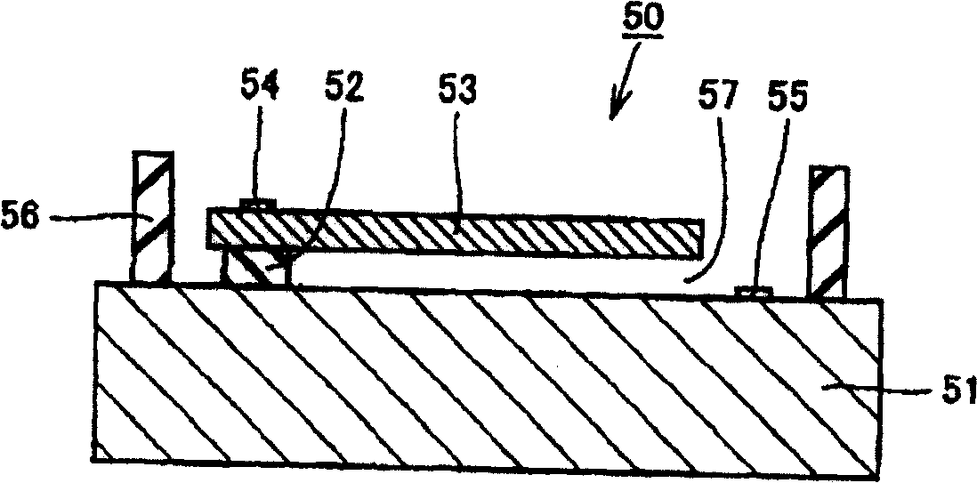
[0046] figure 1 is a plan view showing the semiconductor device in the first embodiment of the present invention, figure 2 is along figure 1 A cross-sectional view of line A-A.

[0047] exist figure 1 Among them, the actuator 50 constituting the semiconductor device has a laminated structure including a substrate 51 , a fixed portion 52 , a conductive layer 53 as a structure, electrode pads 54 and 55 for inputting and outputting signals, and a bank 56 . The conductive layer 53 is formed in a disk shape, and is supported by the fixing portion 52 in a cantilever beam manner, so as to form a gap region 57 with the substrate 51 . The conductive layer 53 moves up and down with the fixing portion 52 as a fulcrum in response to an electric signal supplied to the electrode pads 54 , 55 . In addition, as a structural body, an insulating layer or a semiconductor layer may be used instead of the conductive layer 53 .

[0048] The substrate 51 is formed in a rectangular shape wit...


PUM


Abstract

A semiconductor device, wherein a substrate (51) is formed in a rectangular shape with four sides along dicing lines, and a jetty part (56) is formed to surround all the peripheries of an actuator element (50) and electrode pads (54) and (55) for input / output. The jetty part (56) is formed in a rectangular shape with four sides, and each side thereof is continuously extended parallel with each side of the substrate (51). Since the adhesion of a protective tape (9) can be increased by the jetty part (56), foreign matters (104) produced in dicing can be prevented from adhering to the actuator element (50) and the electrode pads (54) and (55).

Description

technical field [0001] The present invention relates to a semiconductor device, and more particularly to a semiconductor device divided into individual chips by dicing. Background technique [0002] Figure 13 is a schematic diagram of the actuator, (a) shows a plan view, and (b) is a cross-sectional view along line B-B in (a). [0003] exist Figure 13 Among them, the actuator 50 is a laminated structure including a substrate 51 , a fixing portion 52 , a conductive layer 53 and electrode pads 54 , 55 . The conductive layer 53 is formed in a disk shape, and is supported by the fixing portion 52 in a cantilever beam manner, so as to form a gap region 57 with the substrate 51 . The conductive layer 53 moves up and down with the fixing portion 52 as a fulcrum in response to an input electric signal supplied to the electrode pad. [0004] like Figure 14 As shown, when forming a plurality of Figure 13 After executing the components 50 shown, each component is cut and segment...

Claims


Application Information

Patent Timeline
Patent Type & Authority Patents(China)
IPC IPC(8): H01L21/301B81C1/00G01D5/24G01P15/125H01L29/84
Inventor 加川健一八壁正巳
Owner TOKYO ELECTRON LTD
Why Eureka
Try Eureka