Stress sensor chip based on SOI

A stress sensor and insulator technology, applied in semiconductor devices, semiconductor/solid state device testing/measurement, application of piezoresistive material property force measurement, etc. , to achieve the effect of high temperature reliability

Inactive Publication Date: 2008-12-03
TSINGHUA UNIV
View PDF4 Cites 0 Cited by
  • Summary
  • Abstract
  • Description
  • Claims
  • Application Information

AI Technical Summary

Problems solved by technology

However, the use of (100) oriented silicon wafers as stress sensor chips has an important disadvantage, that is, stress sensors based on (100) oriented silicon wafers can only measure four of all six stress components, including three normal stress components. and in-plane shear stress, that is, the other two shear stress components cannot be measured, resulting in the use of (100) silicon wafers as sensor chips cannot achieve the measurement of all stress components
The stress sensor chip based on the (111) crystal silicon wafer can measure all six stress components; but if the sensor chip with the (111) crystal orientation is used instead of the measured chip to be placed in the package, it will be composed of the (111) silicon wafer and (100) The mechanical properties of the silicon wafer are different, resulting in the stress distribution of the (111) sensor chip being completely different from the stress distribution of the (100) tested chip, so it is impossible to accurately reproduce the stress state of the actual (100) chip
[0005] In addition, the use of piezoresistive or MOSFET stress measurement chips fabricated on bulk silicon materials is limited in temperature
This is mainly due to the fact that the insulation of devices on bulk silicon materials mainly relies on the reverse biased pn junction to form isolation and insulation, but in a high temperature working environment, the reverse biased pn junction and substrate leakage leakage current increases significantly, and the reverse bias The insulation ability of the pn junction decreases rapidly, which seriously affects the performance of the sensor

Method used


Image

  • Stress sensor chip based on SOI
  • Stress sensor chip based on SOI
  • Stress sensor chip based on SOI

Examples


Embodiment Construction

[0016] The invention proposes a stress sensor chip based on a silicon-on-insulator chip. The working principle of the present invention will be described below in conjunction with the accompanying drawings.

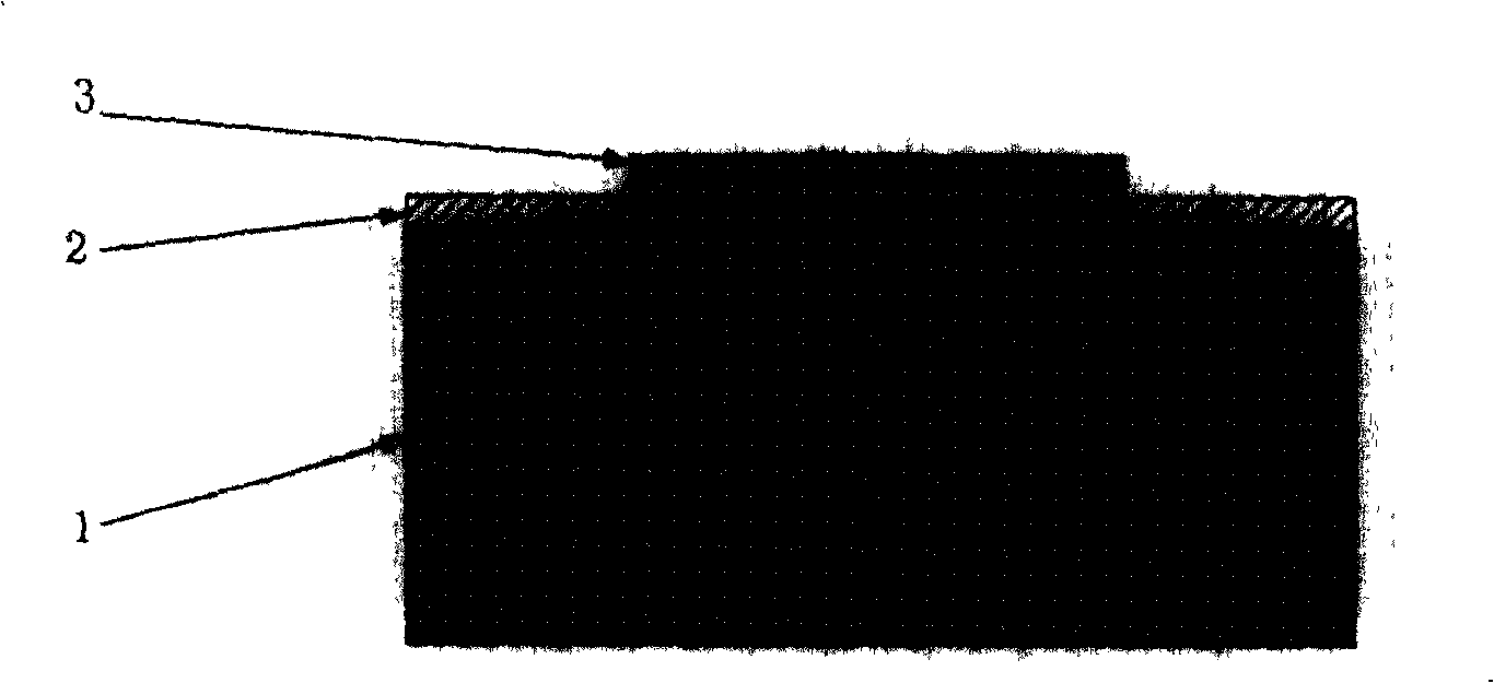
[0017] figure 1 A schematic diagram of the structure of a stress sensor chip on an SOI silicon wafer is shown. exist figure 1 In this method, a silicon dioxide insulating layer 2 is formed on a silicon substrate 1, and a stress-sensitive element layer 3 is formed on the silicon dioxide insulating layer 2. The SOI silicon chip realizes the insulation between the stress-sensitive element layer and the substrate by oxidizing the insulating layer 2, and can still maintain insulation even at high temperatures, ensuring the reliability of the sensor chip. The reverse-biased PN junction realizes the insulation between the stress-sensitive element layer and the substrate, and when the temperature rises, the increase of reverse-bias leakage current will affect the performance o...


PUM

PropertyMeasurementUnit
thicknessaaaaaaaaaa

Abstract

The invention discloses a stress sensor chip based on the silicon of insulator, belonging to the high temperature measurement, and the manufacturing, packaging and measurement technique of integrate circuit. Wherein, the invention makes a silicon oxide insulating barrier on the silicon substrate and makes a stress sensing element layer on the silicon oxide insulating barrier. The advantages of The invention comprises that the sensor chip can measure the stresses of total six directions, and the stress sensor made from SOI substrate avoids the reverse bias PN junction as insulating barrier for keeping insulating ability in high temperature, therefore, it can confirm the operation reliability of sensor chip that it can operate in the high temperature of 600 Deg. C. In addition, the stress sensor chip made from SOI formed by two monocrystalline silicon in different crystallographic direction can realize the stress condition of real integrate circuit chip and accurately measure the total six stress components that the chip bears, when it replaces the circuit tube core to operate the stress measurement.

Description

technical field [0001] The invention belongs to the technical fields of high-temperature mechanical measurement and integrated circuit manufacturing, packaging and measurement. In particular, it relates to a stress sensor chip based on silicon-on-insulator (SOI). Background technique [0002] Although the integration level of integrated circuits is continuously increasing, the area and complexity of integrated circuits are still increasing along with the increasing requirements for functions and performance. The stress of the integrated circuit after packaging will have a huge impact on the reliability and performance of the integrated circuit, especially for the case of large area, small feature size or multi-layer and multi-chip packaging. During the packaging process, chips and adhesives, Stress will be formed between the adhesive and the packaging substrate, causing complex stress distributions after the chip is packaged. These stresses will affect the performance (such...

Claims


Application Information

Patent Timeline
Patent Type & Authority Patents(China)
IPC IPC(8): H01L21/66H01L29/84G01L1/18
Inventor 王喆垚田阔潘立阳胡朝红王建锋刘理天
Owner TSINGHUA UNIV
Why Eureka
Try Eureka