Image display device
An image display device and potential technology, applied in the direction of image/graphic display tubes, discharge tubes, screen tubes, etc., can solve the problems of increased electric field strength, breakdown, etc., to reduce the frame area, reduce the depth, and improve insulation The effect of breakdown voltage
- Summary
- Abstract
- Description
- Claims
- Application Information
AI Technical Summary
Problems solved by technology
Method used
Image

Examples
no. 1 Embodiment
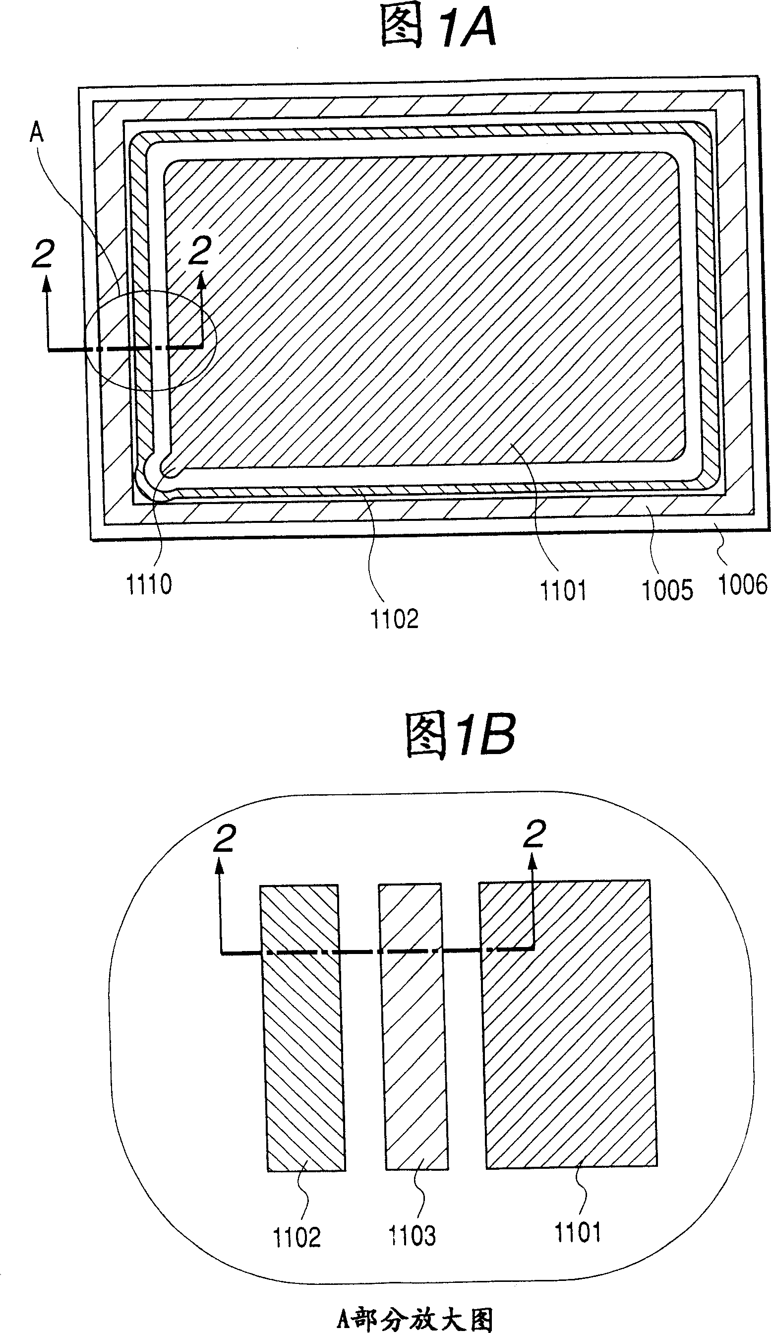
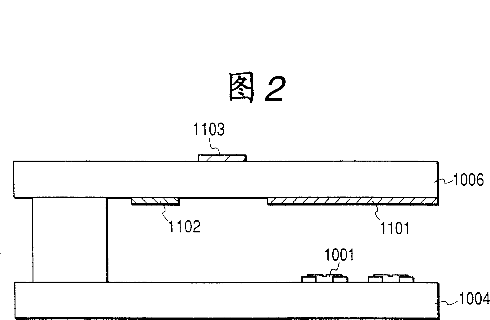
[0058] Hereinafter, a first embodiment of the present invention will be described with reference to FIGS. 1A , 1B and 2 . FIG. 1 is a schematic plan view of an image display device according to a first embodiment of the present invention viewed from a flat panel side. Fig. 2 is a schematic cross-sectional view taken along line 2-2 of Fig. 1A and Fig. 1B .
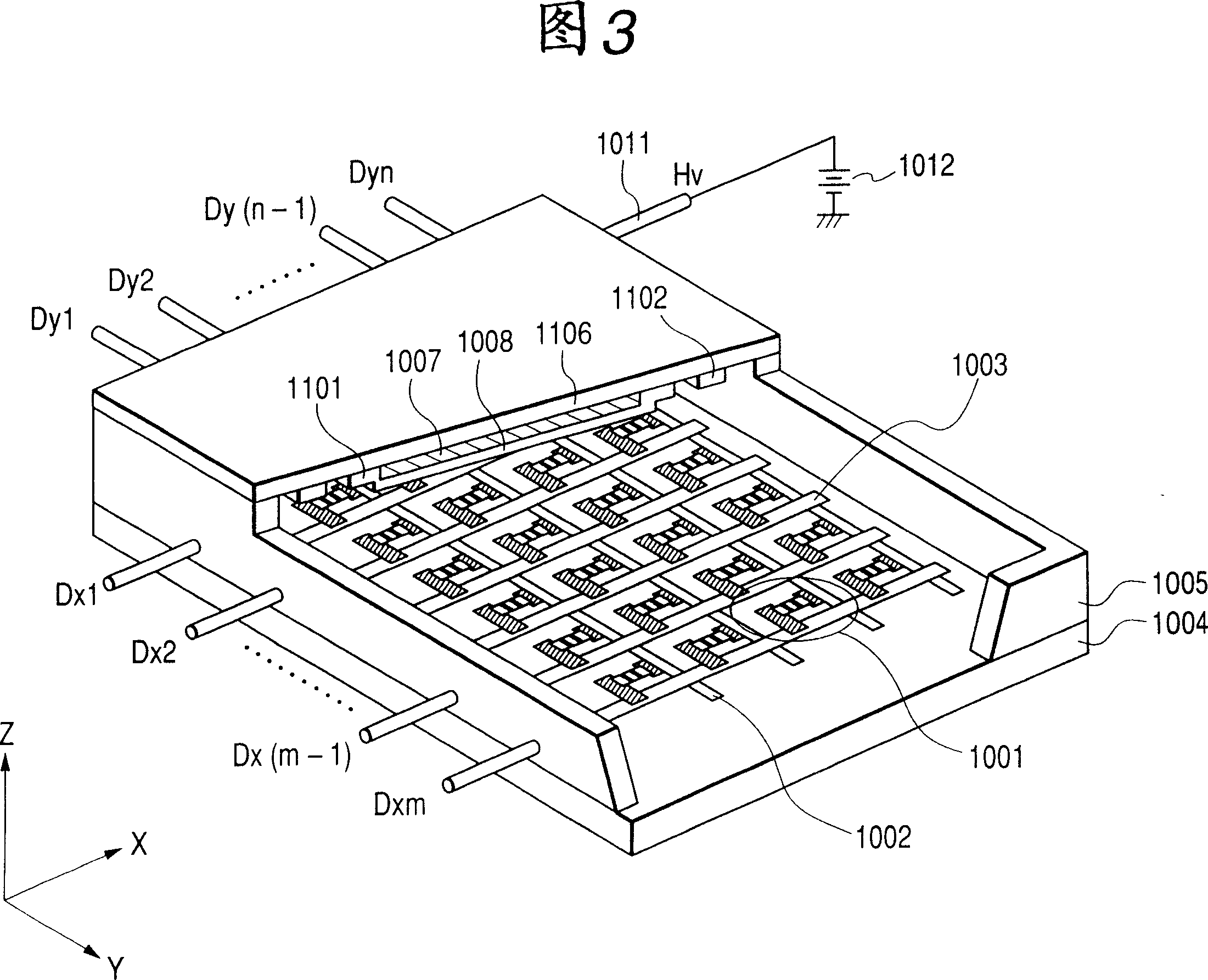
[0059] The flat plate 1006 has an anode electrode 1101 including an image display area, and an anode potential is supplied through a high-voltage extraction part 1110 . A high-voltage lead-in terminal (not shown) is provided on the side of the plate 1006 in the high-voltage take-out portion 1110, and the high-voltage lead-in terminal is connected to a high-voltage power source. In addition, around the anode electrode 1101 and the high-voltage extraction part 1110 on the plate 1006, a first potential regulating member 1102 is provided around which is defined as a ground potential (hereinafter referred to as "GND potential")...
no. 2 Embodiment
[0085] Next, a second embodiment of the present invention will be described with reference to FIG. 5 . Fig. 5 is a schematic sectional view of an image display device according to a second embodiment of the present invention.
[0086] The image display device of the second embodiment is also the same as that of the first embodiment, and the plate 1006 has an anode electrode 1101 enclosing an image area, and a first potential regulating member 1102 arranged around it. Accordingly, compared with the first potential regulating member 1102, the electric field in the outer portion can be relaxed, and breakdown can be prevented from occurring between the side wall or structure (not shown) and the anode electrode. In addition, on the flat plate 1006, the second potential regulating member 1103, which is the characteristic structure of the present invention, is disposed on the back of one of the anode electrode 1101 and the first potential regulating member 1102. Furthermore, the sec...
no. 3 Embodiment
[0090] Next, a third embodiment of the present invention will be described with reference to FIG. 6 . Fig. 6 is a schematic sectional view of an image display device according to a third embodiment of the present invention.
[0091] In this embodiment, as shown in FIG. 6, the second potential regulating member 1103 is formed from the end of the plate 1006 on the atmospheric side of the plate 1006 (the back side of the anode electrode 1101, etc.) to the connection with the first potential regulating member 1102. The metal portion of the display panel frame 1104 is in contact with a region where the orthographic projection of the end portion on the side of the anode electrode 1101 is in contact. That is, the second potential regulating member 1103 is arranged to overlap the entire orthographic projection of the first potential regulating member 1102 . The second potential regulation member 1103, that is, the metal portion of the display panel frame 1104 is regulated as the GND ...
PUM
 Abstract
Description
Claims
Application Information
 - Generate Ideas
- Intellectual Property
- Life Sciences
- Materials
- Tech Scout
- Unparalleled Data Quality
- Higher Quality Content
- 60% Fewer Hallucinations
Browse by: Latest US Patents, China's latest patents, Technical Efficacy Thesaurus, Application Domain, Technology Topic, Popular Technical Reports.
© 2025 PatSnap. All rights reserved.Legal|Privacy policy|Modern Slavery Act Transparency Statement|Sitemap|About US| Contact US: help@patsnap.com