Method of in-situ depositing high dielectric constant Al2O3 and metal film on GaAs substrate
A high dielectric constant and metal film technology, applied in the field of microelectronics, can solve the problems of high production cost, lack of precise control, and many working steps, and achieve the effects of improving work efficiency, saving time, and reducing pollution
- Summary
- Abstract
- Description
- Claims
- Application Information
AI Technical Summary
Problems solved by technology
Method used
Image
Examples
Embodiment 1
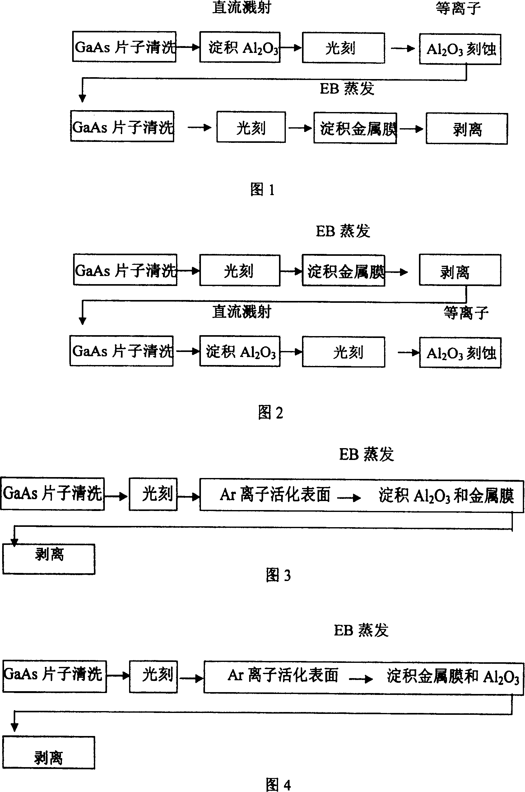
[0094] On the GaAs wafer according to the first evaporation of Al 2 o 3 film, and then evaporate the metal film in sequence. The metal film uses Au, that is, Al 2 o 3 Film evaporation, followed by in-situ evaporation of Au, the specific process is shown in Figure 3;
[0095] In the first step, after cleaning the substrate of the GaAs-based material, it is dried at a temperature of T=120°C for 5 minutes;
[0096] The second step is to photolithographically pattern the cleaned GaAs substrate;
[0097] The third step is to put the photoetched GaAs sheet into the reaction chamber of the EB evaporation table, and firstly evacuate it, and the vacuum degree is required to be 1.8×10 -3 Above Pa, then use argon ions to activate the surface of the GaAs substrate for 20 seconds, so that the vaporized object and the sheet can be firmly adhered, and then carry out the Al 2 o 3 Film evaporation, followed by evaporation of the Au film:
[0098] (1)Al 2 o 3 Film Evaporation Process C...
Embodiment 2
[0114] On GaAs-based materials, first evaporate Al 2 o 3 film, and then evaporate the metal film, the metal film uses AL, that is, Al first 2 o 3 After AL is evaporated in situ, the specific process refers to Figure 3 as follows:
[0115] In the first step, after cleaning the substrate of the GaAs-based material, it is dried at a temperature of T=120°C for 5 minutes;
[0116] The second step is to photolithographically pattern the cleaned GaAs substrate;
[0117] In the third step, put the photolithographic GaAs wafer into the reaction chamber of the EB evaporation table, and firstly evacuate it at 1.8×10 -3 Above Pa; then use argon ions to activate the surface of the GaAs substrate for 20 seconds, so that the vaporized object and the sheet can be firmly adhered, and then carry out Al in accordance with the following process conditions 2 o 3 Film evaporation, and then evaporation of the Al film:
[0118] (1)Al 2 o 3 Film Evaporation Process Conditions
[0119] a, wil...
Embodiment 3
[0132] On the GaAs substrate, the metal film is evaporated first, and then the Al 2 o 3 Evaporation, the metal film uses Au, Ge, Ni, that is, Au / Ge / Ni first, then Al 2 o 3 In-situ evaporation, its specific process is as follows with reference to Figure 4:
[0133] In the first step, after cleaning the substrate of the GaAs-based material, it is dried at a temperature of T=120°C for 5 minutes;
[0134] The second step is to photolithographically pattern the cleaned GaAs substrate;
[0135] In the third step, put the photolithographic GaAs wafer into the reaction chamber of the EB evaporation table, and firstly evacuate it at 1.8×10 -3 Above Pa; then use argon ions to activate the surface of the GaAs substrate for 20 seconds, so that the object to be evaporated and the chip are firmly adhered, and then according to the following process conditions, the Au metal film is first evaporated, then the Ge metal film is evaporated, and then the Ni metal film is evaporated. Evaporat...
PUM
| Property | Measurement | Unit |
|---|---|---|
| particle size | aaaaa | aaaaa |
Abstract
Description
Claims
Application Information
 - Generate Ideas
- Intellectual Property
- Life Sciences
- Materials
- Tech Scout
- Unparalleled Data Quality
- Higher Quality Content
- 60% Fewer Hallucinations
Browse by: Latest US Patents, China's latest patents, Technical Efficacy Thesaurus, Application Domain, Technology Topic, Popular Technical Reports.
© 2025 PatSnap. All rights reserved.Legal|Privacy policy|Modern Slavery Act Transparency Statement|Sitemap|About US| Contact US: help@patsnap.com


