Method for manufacturing semiconductor device to facilitate peeling of a supporting substrate bonded to a semiconductor wafer
a manufacturing method and technology of a supporting substrate, applied in the field of manufacturing a semiconductor device, can solve the problems of the limitation of the taiko process in manufacturing ultrathin devices with thickness, and achieve the effect of preventing chipping or breaking of the wafer and easy peeling of the supporting substra
- Summary
- Abstract
- Description
- Claims
- Application Information
AI Technical Summary
Benefits of technology
Problems solved by technology
Method used
Image
Examples
embodiment 1
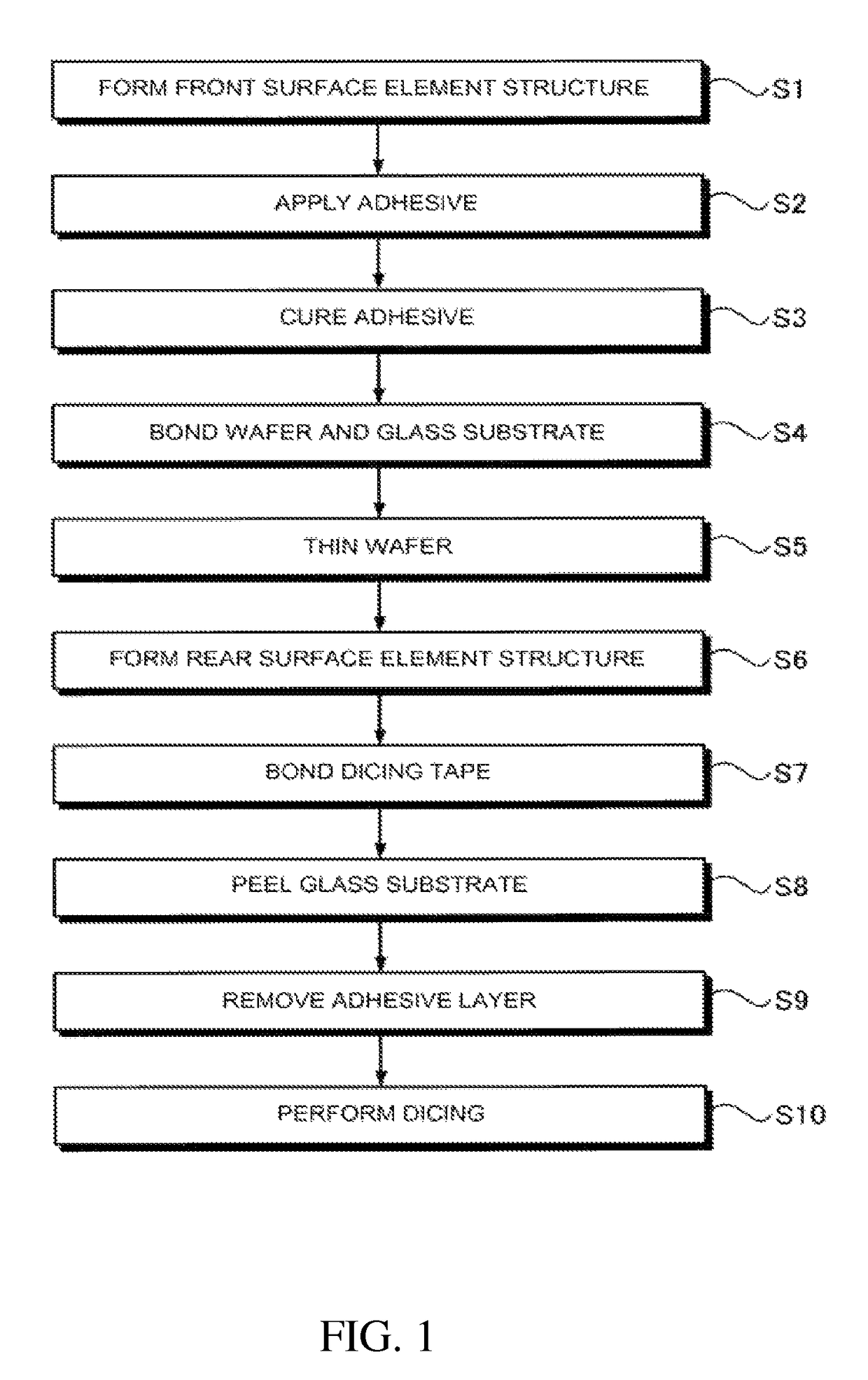
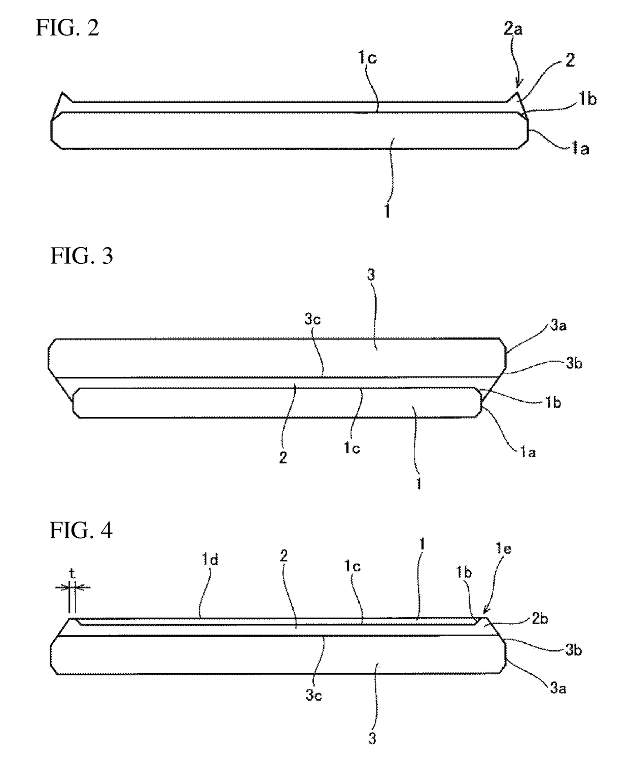
[0049]A method for manufacturing a semiconductor device according to Embodiment 1 will be described. FIG. 1 is a flowchart illustrating the outline of the method for manufacturing a semiconductor device according to Embodiment 1. FIGS. 2 to 5 are cross-sectional views illustrating states during manufacture in the flowchart illustrated in FIG. 1. First, processing is performed on a front surface of a general wafer 1 to form a front surface element structure (not illustrated) on a front surface (first main surface) 1c of the wafer 1 (Step S1). Then, an adhesive 2 is applied onto the entire front surface 1c of the wafer 1 by a coater (Step S2). In Step S2, for example, a spinning method which rotates the wafer 1 fixed to a stage at a high speed to spread the adhesive 2 applied onto the front surface 1c of the wafer 1 using centrifugal force is used.
[0050]The upper and lower ends (corners: hereinafter, referred to as chamfered portions) 1b of a side surface 1a of the wafer 1 are chamfer...
embodiment 2
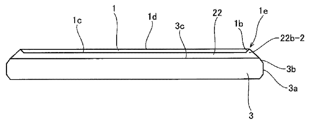
[0065]Next, a method for manufacturing a semiconductor device according to Embodiment 2 will be described. FIG. 6 is a flowchart illustrating the outline of the method for manufacturing the semiconductor device according to Embodiment 2. FIGS. 7 to 9 are cross-sectional views illustrating states during manufacture in the flowchart illustrated in FIG. 6. The method for manufacturing the semiconductor device according to Embodiment 2 differs from the method for manufacturing the semiconductor device according to Embodiment 1 in that a process (Step S21) of removing an extra portion of an adhesive layer 22 is added between Step S5 and Step S6. That is, in Embodiment 2, when a wafer 1 and a glass substrate 3 are bonded to each other and a chamfered portion 3b and a side surface 3a of the glass substrate 3 are covered by a protruding portion in the outer circumference of an adhesive layer 22, the extra portion of the adhesive layer 22 is removed.
[0066]Specifically, first, similarly to Em...
embodiment 3
[0071]Next, a method for manufacturing a semiconductor device according to Embodiment 3 will be described. FIG. 11 is a flowchart illustrating the outline of the method for manufacturing the semiconductor device according to Embodiment 3. FIGS. 12 and 13 are cross-sectional views illustrating a state during manufacture in the flowchart illustrated in FIG. 11. The method for manufacturing the semiconductor device according to Embodiment 3 differs from the method for manufacturing the semiconductor device according to Embodiment 1 in that a process (Step S31) of removing an extra portion of an adhesive layer 32 is added between Step S6 and Step S7. That is, in Embodiment 3, similarly to Embodiment 2, when a wafer 1 and a glass substrate 3 are bonded to each other and a chamfered portion 3b and a side surface 3a of the glass substrate 3 are covered by a protruding portion in the outer circumference of an adhesive layer 32, the extra portion of the adhesive layer 32 is removed.
[0072]Spe...
PUM
| Property | Measurement | Unit |
|---|---|---|
| thickness | aaaaa | aaaaa |
| angle | aaaaa | aaaaa |
| size | aaaaa | aaaaa |
Abstract
Description
Claims
Application Information
 - R&D
- Intellectual Property
- Life Sciences
- Materials
- Tech Scout
- Unparalleled Data Quality
- Higher Quality Content
- 60% Fewer Hallucinations
Browse by: Latest US Patents, China's latest patents, Technical Efficacy Thesaurus, Application Domain, Technology Topic, Popular Technical Reports.
© 2025 PatSnap. All rights reserved.Legal|Privacy policy|Modern Slavery Act Transparency Statement|Sitemap|About US| Contact US: help@patsnap.com


