Eureka AIR delivers breakthrough ideas for toughest innovation challenges, trusted by R&D personnel around the world.

Ternary tungsten boride nitride films and methods for forming same

a technology of tungsten boride nitride and nitride, which is applied in the direction of coatings, basic electric elements, chemistry apparatuses and processes, etc., can solve the problems of preventing these materials from being used together in semiconductor devices, and achieve excellent thermal stability, good adhesion to oxides, and tunable resistivity. good

Active Publication Date: 2018-05-15
LAM RES CORP
View PDF48 Cites 7 Cited by
  • Summary
  • Abstract
  • Description
  • Claims
  • Application Information

AI Technical Summary

Benefits of technology

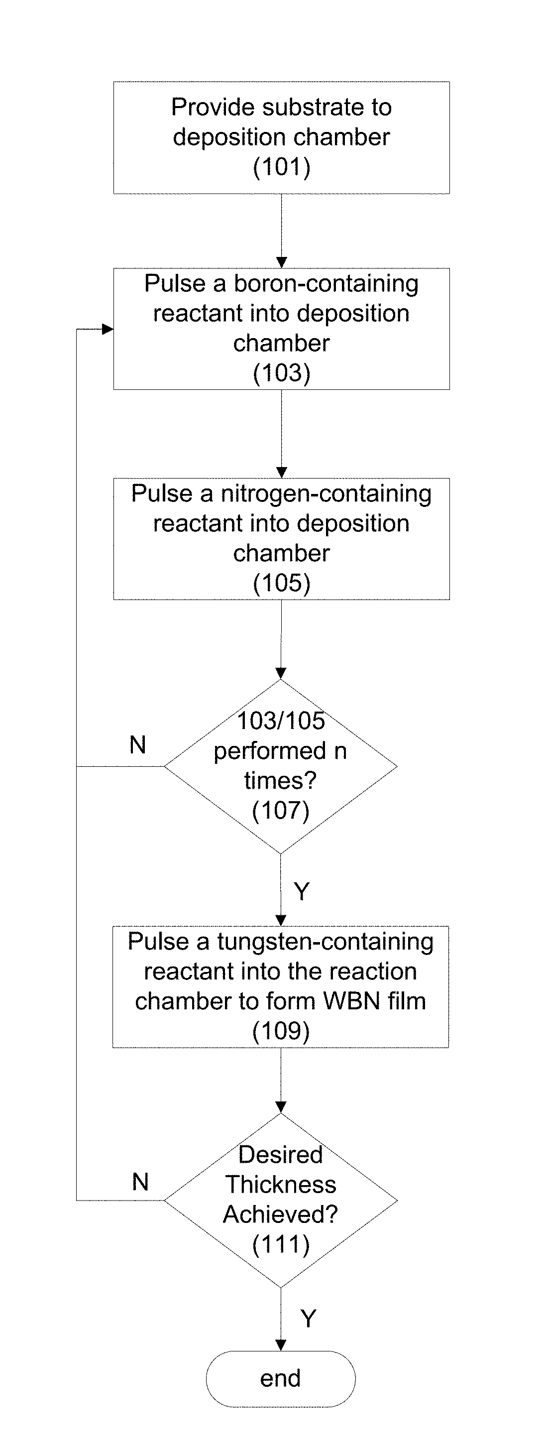
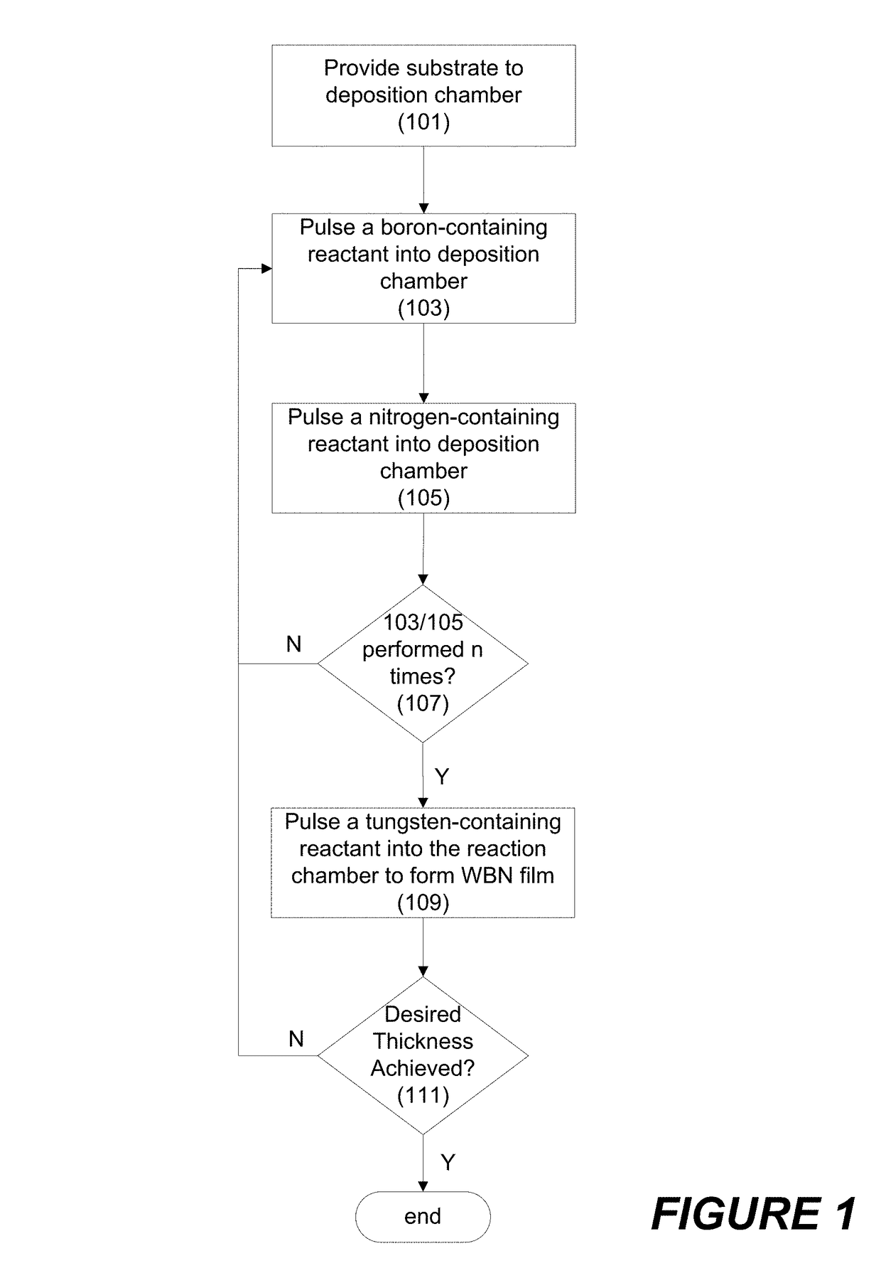
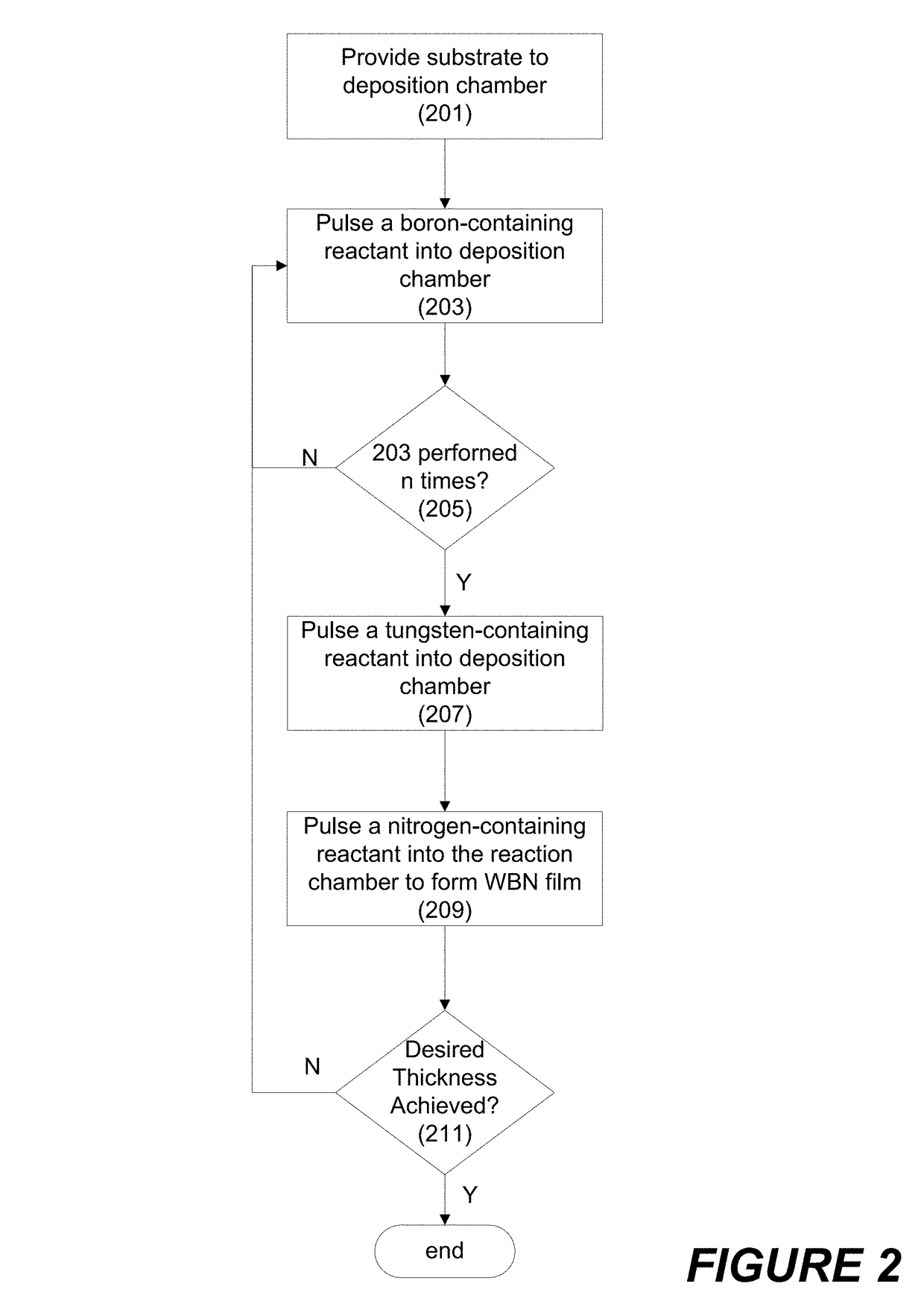
[0004]Ternary tungsten boride nitride (WBN) thin films and related methods of formation are provided. The films have excellent thermal stability, tunable resistivity and good adhesion to oxides. Methods of forming the films can involve thermal atomic layer deposition (ALD) processes in which boron-containing, nitrogen-containing and tungsten-containing reactants are sequentially pulsed into a reaction chamber to deposit the WBN films. In some embodiments, the processes include multiple cycles of boron-containing, nitrogen-containing and tungsten-containing reactant pulses, with each cycle including multiple boron-containing pulses.

Problems solved by technology

Problems regarding the use of low resistivity tungsten layers with tungsten nitride layers, however, have prevented these materials from being used together in semiconductor devices.

Method used


Image

  • Ternary tungsten boride nitride films and methods for forming same
  • Ternary tungsten boride nitride films and methods for forming same
  • Ternary tungsten boride nitride films and methods for forming same

Examples


Embodiment Construction

Introduction

[0012]In the following description, numerous specific details are set forth in order to provide a thorough understanding of the invention, which pertains to tungsten boride nitride films and methods of forming the same. Modifications, adaptations or variations of specific methods and of structures shown herein will be apparent to those skilled in the art and are within the scope of this invention.

[0013]Resistivity is an intrinsic property of a material and a measurement of a material's resistance to the movement of charge through the material. High or low resistivity materials can be used for different applications. For example, low resistivity metal layers in integrated circuits minimize power losses. High resistivity metal layers may be used as heater elements for phase change memory or other applications.

[0014]In one example, tungsten layers may be used as low resistivity electrical connections in the form of horizontal interconnects, vias between adjacent metal layer...


PUM

PropertyMeasurementUnit
temperatureaaaaaaaaaa

Abstract

Ternary tungsten boride nitride (WBN) thin films and related methods of formation are provided. The films are have excellent thermal stability, tunable resistivity and good adhesion to oxides. Methods of forming the films can involve thermal atomic layer deposition (ALD) processes in which boron-containing, nitrogen-containing and tungsten-containing reactants are sequentially pulsed into a reaction chamber to deposit the WBN films. In some embodiments, the processes include multiple cycles of boron-containing, nitrogen-containing and tungsten-containing reactant pulses, with each cycle including multiple boron-containing pulses.

Description

CROSS-REFERENCE TO RELATED CASES[0001]This application claims benefit under 35 USC § 119(e) of the following applications: U.S. Provisional Patent Application No. 61 / 676,123, filed Jul. 26, 2012 and U.S. Provisional Patent Application No. 61 / 697,775, filed Sep. 6, 2012. Both of these applications are incorporated herein by reference in their entireties.BACKGROUND[0002]Resistivity is an intrinsic property of a material and a measurement of a material's resistance to the movement of charge through the material. High or low resistivity materials can be used for different applications. For example, low resistivity metal layers in integrated circuits minimize power losses. High resistivity metal layers may be used as heater elements for phase change memory or other applications.[0003]In one example, tungsten layers may be used as low resistivity electrical connections in the form of horizontal interconnects, vias between adjacent metal layers, and contacts between a first metal layer and...

Claims


Application Information

Patent Timeline
Patent Type & Authority Patents(United States)
IPC IPC(8): C23C16/30C01B35/14H01L23/522H01L21/285C23C16/455H01L45/00H01L23/532H01L21/768C23C16/34
CPCC01B35/146C23C16/30C23C16/342C23C16/45531H01L21/28562H01L21/76843H01L21/76876H01L23/5226H01L23/53266H01L45/06H01L45/126H01L45/16H01L2924/0002H01L2924/00H10N70/8413H10N70/231H10N70/011C23C30/00C23C16/44
Inventor LEI, WEIGAO, JUWEN
Owner LAM RES CORP
Why Eureka
Eureka Blog
Learn More