Electronic component
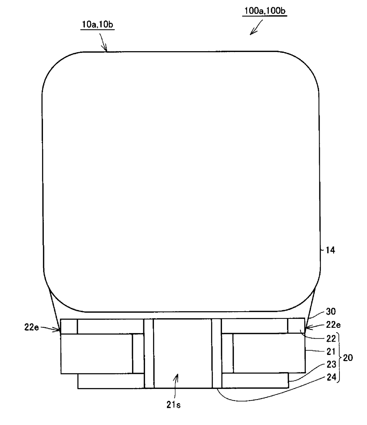
a technology of electronic components and components, applied in the field of electronic components, can solve problems such as and achieve the effect of significantly reducing or preventing failures in mounting of electronic components due to electrode burrs on the substrate terminal
- Summary
- Abstract
- Description
- Claims
- Application Information
AI Technical Summary
Benefits of technology
Problems solved by technology
Method used
Image
Examples
first preferred embodiment
[0052]First, a capacitor element as an example of an electronic element included in an electronic component according to a first preferred embodiment of the present invention will be described. The electronic element is not limited to the capacitor element and may be an inductor element, a thermistor element, a piezoelectric element, a semiconductor element, or the like.
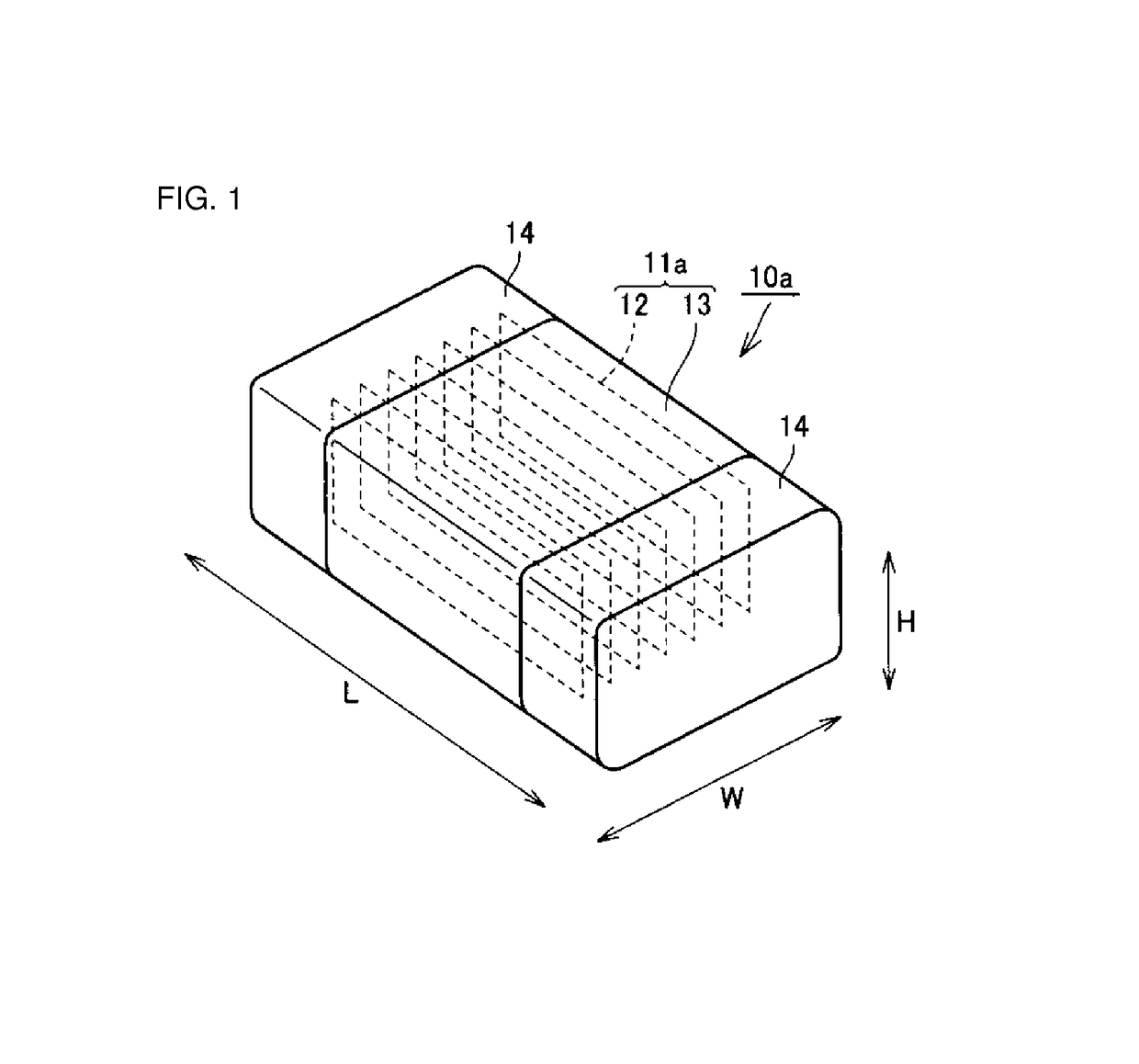
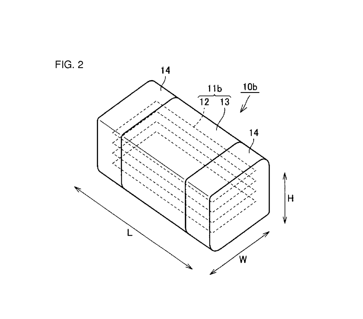
[0053]FIG. 1 is a perspective view illustrating a first structure of the capacitor element included in the electronic component according to the first preferred embodiment of the present invention. FIG. 2 is a perspective view illustrating a second structure of the capacitor element included in the electronic component according to the first preferred embodiment of the present invention. In FIGS. 1 and 2, a lengthwise direction L of the capacitor element, a width direction W of the capacitor element, and a height direction H of the capacitor element are illustrated.
[0054]As illustrated in FIG. 1, a capacitor element ...
second preferred embodiment
[0121]FIG. 14 is an exploded perspective view illustrating the electronic component according to the second preferred embodiment of the present invention. In FIG. 14, a conductor included in the electronic component is not illustrated.
[0122]As illustrated in FIG. 14, in a substrate terminal 20b included in the electronic component according to the second preferred embodiment of the present invention, the length of each adjacent portion 22e in the lengthwise direction of the insulating substrate 21 is preferably equal or substantially equal to a maximum length L1 of other portions of each mounting electrode 22.
[0123]FIG. 15 is a view illustrating a mother substrate as a base of a substrate terminal included in the electronic component according to the present preferred embodiment when seen from the first main surface side. FIG. 16 is a view illustrating a cut mother substrate when seen from the first main surface side in the present preferred embodiment.
[0124]As illustrated in FIGS. ...
third preferred embodiment
[0129]FIG. 17 is a view illustrating a mother substrate as a base of a substrate terminal included in the electronic component according to the third preferred embodiment of the present invention when seen from the second main surface side. FIG. 18 is a view illustrating a cut mother substrate when seen from the second main surface side in the present preferred embodiment.
[0130]As illustrated in FIGS. 17 and 18, a mother substrate 200c is cut along the cut lines CL1 and CL2 as virtual lines so as to be individual substrate terminals 20c.
[0131]As illustrated in FIG. 17, in the mother substrate 200c as the base of the substrate terminal included in an electronic component according to the present preferred embodiment, a wiring pattern on the second main surface 210b has a configuration such that the plurality of electrodes 230 are coupled by coupling portions 230e as in the wiring pattern on the first main surface 210a.
[0132]As illustrated in FIGS. 17 and 18, in the second main surf...
PUM
 Abstract
Description
Claims
Application Information
 - R&D
- Intellectual Property
- Life Sciences
- Materials
- Tech Scout
- Unparalleled Data Quality
- Higher Quality Content
- 60% Fewer Hallucinations
Browse by: Latest US Patents, China's latest patents, Technical Efficacy Thesaurus, Application Domain, Technology Topic, Popular Technical Reports.
© 2025 PatSnap. All rights reserved.Legal|Privacy policy|Modern Slavery Act Transparency Statement|Sitemap|About US| Contact US: help@patsnap.com


