
Method for producing a microelectronic device

a microelectronic and microelectronic technology, applied in the direction of semiconductor devices, basic electric elements, electrical apparatus, etc., can solve the problems of inability to contain, inability to meet the requirements of the structure inability to overcome the visible inability of the transistor of the metal-oxide-semiconductor (mos) to achieve the effect of reducing the cost of the solid silicon type, less roughness, and reliable thickness

Active Publication Date: 2018-03-13
COMMISSARIAT A LENERGIE ATOMIQUE ET AUX ENERGIES ALTERNATIVES
View PDF23 Cites 0 Cited by
  • Summary
  • Abstract
  • Description
  • Claims
  • Application Information

AI Technical Summary

Benefits of technology

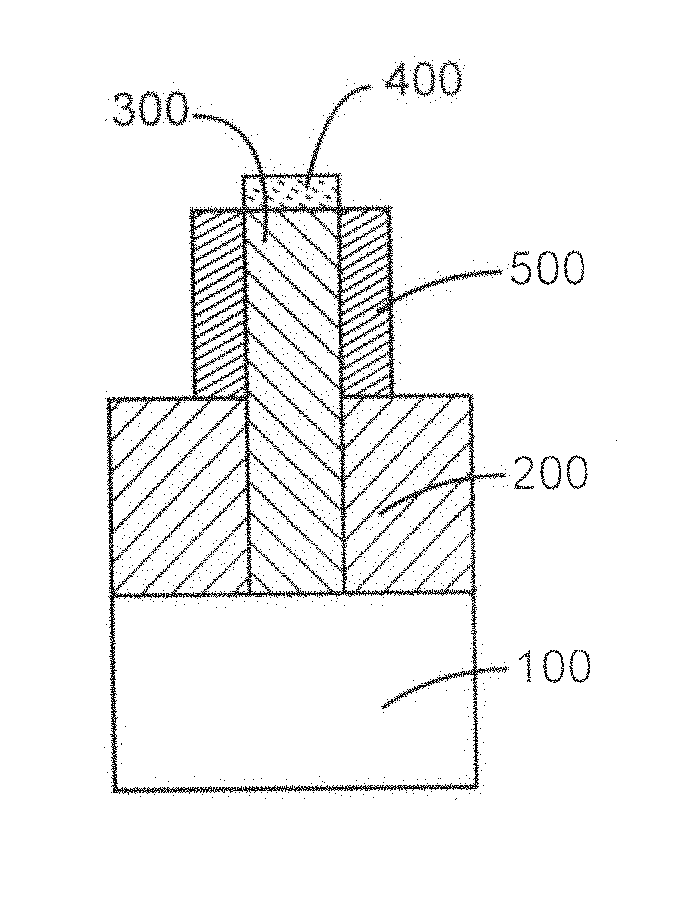
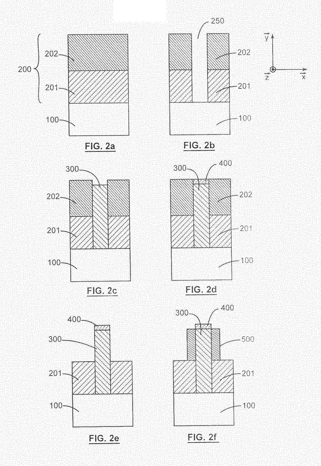
[0017]Thus the present invention makes it possible to produce, in a simple and reproducible manner, from a crystalline substrate formed from the first material, at least one crystalline epitaxial layer made from a second material that is, according to an advantageous embodiment, different from the first material of the substrate.
[0032]The channels obtained may thus have a very reliable thickness, a thickness taken in a plane parallel to the plane in which the substrate mainly lies.

Problems solved by technology

However, this race for integration is on the point of coming up against limits of a physical and technological nature that transistors of the metal-oxide-semiconductor (MOS) on solid silicon type will visibly not manage to overcome.
Furthermore, architecture on solid silicon will not make it possible to contain, beyond a certain integration threshold, the bidimensional electrostatic forces and certain quantal effects detrimental to the vertical field effect caused by the gate.
These solid substrates other than silicon have the drawbacks of their cost and their incompatibility in terms of size with equipment developed for the latest generations of silicon components (300 mm, 450 mm in preparation).
However, this approach comes up against the high disparity in lattice parameter between the main materials of interest and silicon.
Under these circumstances, obtaining a continuous epitaxial layer (over the entire host substrate), comprising a minimum of crystalline defects, makes it necessary to have recourse to thick intermediate buffer layers, making the approach particularly expensive without being completely effective.
Nevertheless, this approach has several limits.
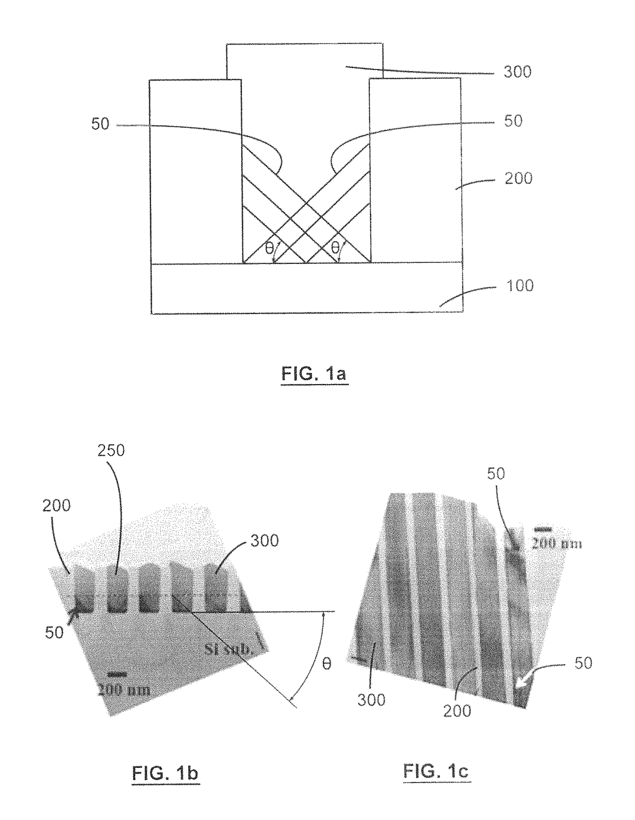
In addition, obtaining dense patterns of the layer 300 of germanium is directly limited by the minimum photorepetition pitch.
Moreover, an additional drawback lies in the width of the epitaxed channel formed by the layer 300 of germanium that is directly subjected to the variations imposed by the steps of formation of the trenches 250; said trenches 250 being produced by photolithography and / or etching for example.

Method used


Image

  • Method for producing a microelectronic device
  • Method for producing a microelectronic device
  • Method for producing a microelectronic device

Examples


Embodiment Construction

[0054]Before beginning a detailed review of embodiments of the invention, optional features, which may optionally be used in association or alternatively, are stated below.

[0055]It is stated first of all that the invention relates to a method for producing a crystalline layer from a crystalline substrate.

[0056]Preferentially, the growth of the buffer layer comprises an epitaxial growth from the substrate. Particularly advantageously, the epitaxial growth makes it possible to obtain a layer the material of which is of better crystalline quality, thereby comprising a smaller number of dislocations. Epitaxial growth techniques are preferably chosen from chemical vapour deposition (CVD) techniques or molecular beam epitaxy (MBE); these techniques frequently being used in industry.

[0057]According to one alternative, the growth of the buffer layer comprises a deposition of said layer followed by a crystallisation annealing. For this type of deposition, chemical vapour deposition can advan...


PUM


Abstract

A crystalline layer is produced from a crystalline substrate made from a first material on which a masking layer has previously been deposited; the masking layer containing at least one trench forming an access to the substrate, by:forming a crystalline buffer layer situated at least partly in the trench in the masking layer, extending from the substrate and forming a projection beyond the masking layer so that an upper part of the lateral flanks of said buffer layer is left uncovered, the formation step comprising a growth of the buffer layer from the substrate, andforming a crystalline epitaxial layer in a second material, different from the material of the buffer layer, by growth from said upper part of the lateral flanks of the buffer layer left uncovered.

Description

FIELD OF THE INVENTION[0001]The present invention relates to devices for microelectronics and methods for producing same. It relates in particular to semiconductors having high mobilities (for example based on carbon, germanium, alloys of elements in group III-V, or constrained silicon), presented as alternatives to silicon for certain applications in ultimate technological nodes.TECHNOLOGICAL BACKGROUND[0002]In the field of microelectronics, the constant reduction in the surface area of silicon occupied by the components has up until now made it possible to maintain the race for integration at a rate decreed by Moore's law, which provides that the number of transistors per integrated circuit doubles approximately every 18 to 24 months. However, this race for integration is on the point of coming up against limits of a physical and technological nature that transistors of the metal-oxide-semiconductor (MOS) on solid silicon type will visibly not manage to overcome. Furthermore, arch...

Claims


Application Information

Patent Timeline
Patent Type & Authority Patents(United States)
IPC IPC(8): H01L21/8234H01L29/66H01L21/02H01L29/10H01L29/20H01L29/78H01L29/205H01L21/311H01L21/324H01L29/04H01L29/165H01L21/31H01L21/308H01L21/306
CPCH01L29/1054H01L29/7849H01L21/0254H01L21/02381H01L21/02452H01L21/02458H01L21/02463H01L21/02532H01L21/02535H01L21/02546H01L21/02598H01L21/02636H01L21/02639H01L21/3081H01L21/30604H01L21/30612H01L21/31H01L21/31116H01L21/324H01L21/3245H01L21/823431H01L29/04H01L29/165H01L29/2003H01L29/205H01L29/66795H01L29/785H01L21/0245
Inventor AUGENDRE, EMMANUELBARON, THIERRY
Owner COMMISSARIAT A LENERGIE ATOMIQUE ET AUX ENERGIES ALTERNATIVES
Learn More