Monolithic three-axis linear magnetic sensor and manufacturing method thereof
a three-axis linear magnetic sensor and manufacturing method technology, applied in the field of linear magnetic sensors, can solve the problem of unnecessary use of algorithms for computation, and achieve the effects of increasing the sensitivity of the z-axis sensor, reducing the width lx and increasing the thickness lz of the z ferromagnetic flux guid
- Summary
- Abstract
- Description
- Claims
- Application Information
AI Technical Summary
Benefits of technology
Problems solved by technology
Method used
Image
Examples
embodiment 1
[0072
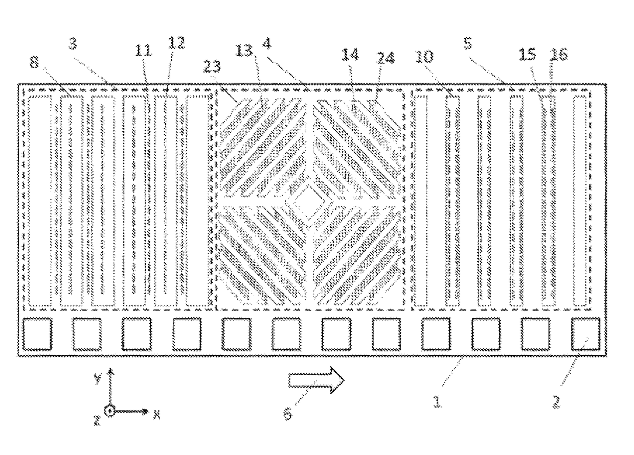
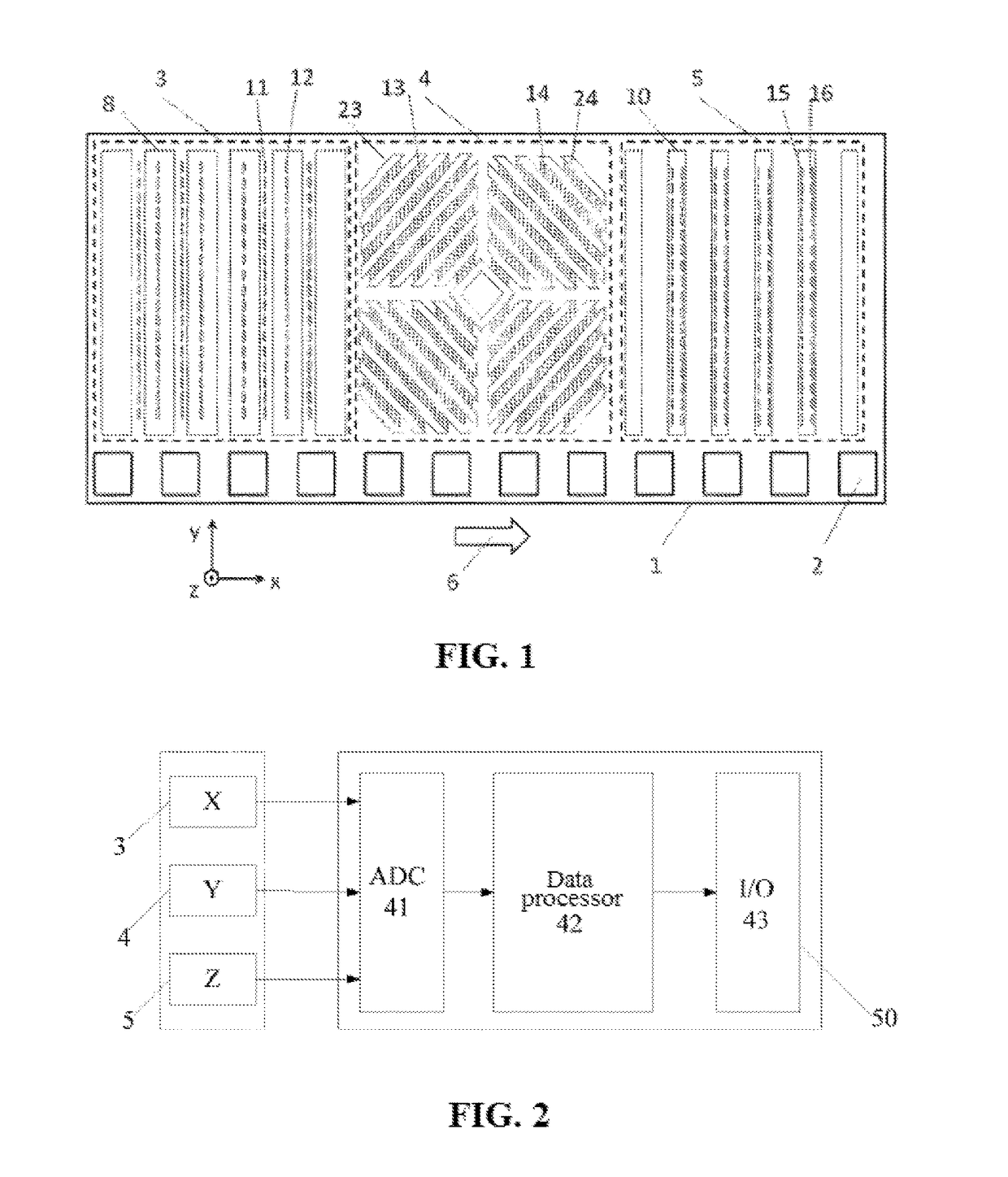
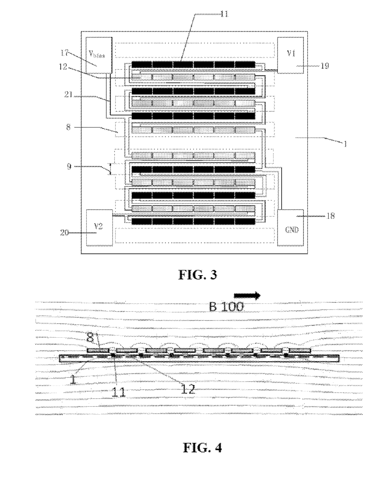
[0073]FIG. 1 is a schematic structural diagram of a monolithic three-axis linear magnetic sensor in the present invention in an XY plane. The sensor includes a substrate 1, and the substrate 1 is integrated thereon with an X-axis sensor 3, a Y-axis sensor 4, a Z-axis sensor 5 and a plurality of bonding pads 2 for input and output. The X-axis sensor 3 includes sensing element series 11, reference element series 12 and X ferromagnetic flux guides 8, wherein the reference element series 12 are placed beneath the X ferromagnetic flux guides 8, and the sensing element series 11 are placed at a gap between the adjacent two of the X ferromagnetic flux guides 8. The sensing element series 11 and the reference element series 12 are each formed by electrically connecting one or more identical magnetoresistive sensing elements. The Y-axis sensor 4 includes Y ferromagnetic flux guides 23, 24 and magnetoresistive sensing elements 13, 14, wherein the magnetoresistive sensing elements 13 are ...
embodiment 2
[0110
[0111]FIG. 20 is a method for manufacturing a monolithic three-axis linear magnetic sensor in the present invention, and the method includes the following steps:
[0112](1) depositing a magnetoresistive material thin film stack on a wafer, and setting a magnetization direction of a pinned layer on the magnetoresistive material thin film stack by using a related process, preferably setting the magnetization direction of the pinned layer to be along the same direction by thermal annealing in a magnetic field, and setting electrical properties and magnetic properties thereof, including impedance, threshold voltage, hysteresis, anisotropy, saturated magnetic field and so on, wherein the magnetic properties are specific to the pinned layer and a free layer, while the electrical properties are specific to a tunnel junction. In the magnetoresistive material thin film stack, the pinned layer is pinned by using an antiferromagnetic material having a blocking temperature of TB1, and the fr...
PUM
 Abstract
Description
Claims
Application Information
 - R&D
- Intellectual Property
- Life Sciences
- Materials
- Tech Scout
- Unparalleled Data Quality
- Higher Quality Content
- 60% Fewer Hallucinations
Browse by: Latest US Patents, China's latest patents, Technical Efficacy Thesaurus, Application Domain, Technology Topic, Popular Technical Reports.
© 2025 PatSnap. All rights reserved.Legal|Privacy policy|Modern Slavery Act Transparency Statement|Sitemap|About US| Contact US: help@patsnap.com


