Array substrate for fringe field switching mode liquid crystal display device and method of fabricating the same

a fringe field switching mode and liquid crystal display technology, applied in semiconductor devices, optics, instruments, etc., can solve the problems of ips mode lcd device having disadvantages in aperture ratio and transmissivity, poor viewing angle of lcd device, increase production cost, etc., to reduce mask process and improve aperture ratio

Active Publication Date: 2017-09-19
LG DISPLAY CO LTD
View PDF8 Cites 0 Cited by
  • Summary
  • Abstract
  • Description
  • Claims
  • Application Information

AI Technical Summary

Benefits of technology

[0031]An object of the present invention is to provide an array substrate for an FFS mode LCD device having improved aperture ratio.
[0032]Another object of the present invention is to provide an array substrate for an FFS mode LCD device being capable of reducing mask processes.

Problems solved by technology

However, since the related art LCD device uses a vertical electric field, the LCD device has a bad viewing angle.
Unfortunately, the IPS mode LCD device has disadvantages in aperture ratio and transmissivity.
However, since the mask process includes many steps, such as a depositing step, an exposing step, a developing step, an etching step, and so on, the mask process causes increase of production costs.
As explained above, the array substrate for the related art FFS mode LCD device requires the explained seven mask process, which may result in a disadvantage on production costs as the number of mask processes increase.

Method used


Image

  • Array substrate for fringe field switching mode liquid crystal display device and method of fabricating the same
  • Array substrate for fringe field switching mode liquid crystal display device and method of fabricating the same
  • Array substrate for fringe field switching mode liquid crystal display device and method of fabricating the same

Examples


Embodiment Construction

[0048]Reference will now be made in detail to embodiments of the present invention, examples of which are illustrated in the accompanying drawings. The same reference numbers may be used throughout the drawings to refer to the same or like parts.

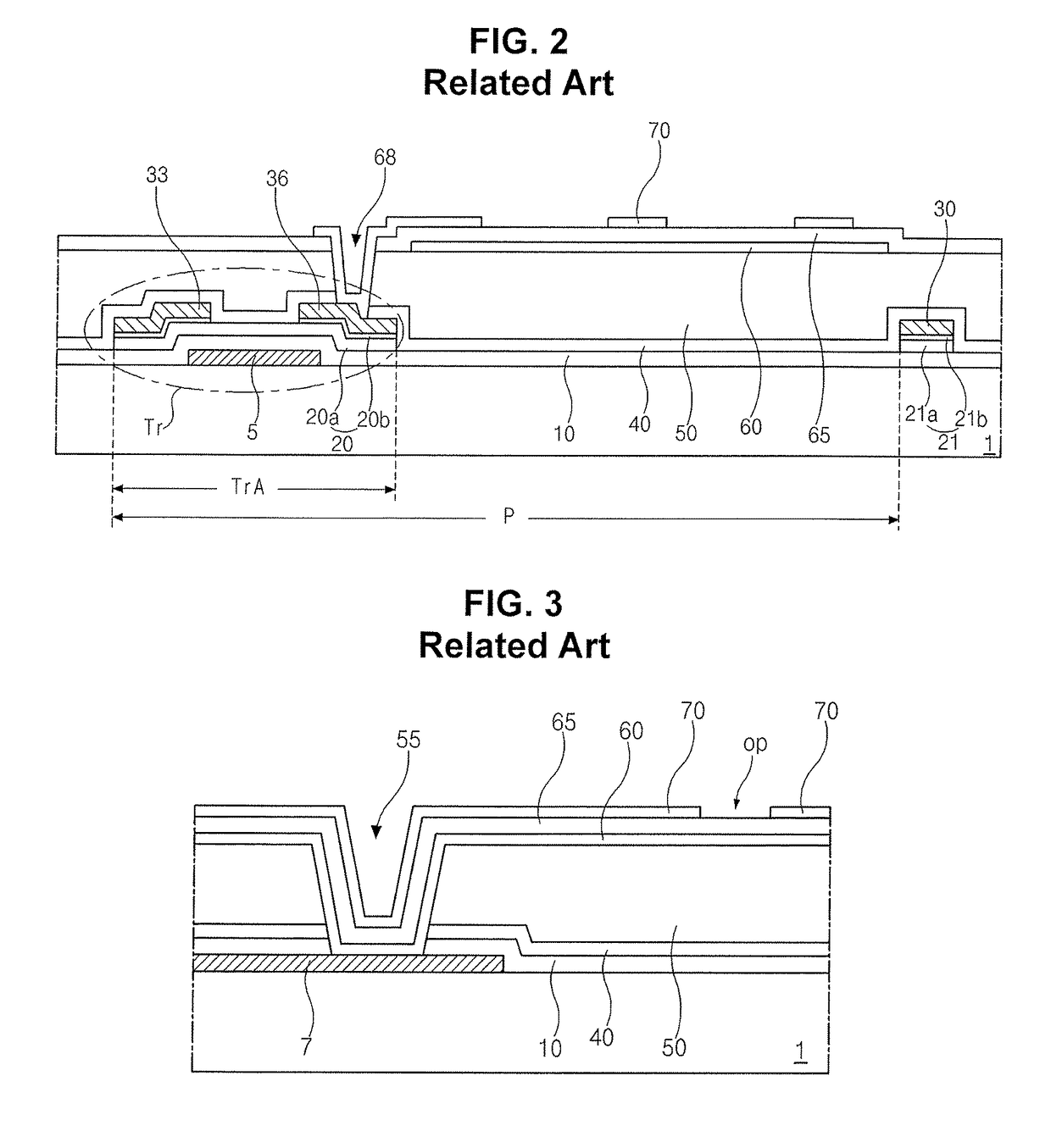
[0049]As described above, the array substrate of the related art FFS mode LCD device is fabricated by the seven mask process with increased production costs. To reduce the cost of mask processes, the drain contact hole may be formed in the third mask process. However, as the drain electrode is exposed through the drain contact hole during the fourth and fifth mask processes, particles may be stacked on the drain electrode. In this case, a contact problem between the pixel electrode and the drain electrode can be generated.

[0050]In addition, when a problem occurs in the fifth mask process for forming the common electrode with the drain contact hole, an electrical short problem between the common electrode and the pixel and drain electrodes ca...


PUM

PropertyMeasurementUnit
thicknessaaaaaaaaaa
sizeaaaaaaaaaa
optical anisotropyaaaaaaaaaa

Abstract

An array substrate for a liquid crystal display (LCD) device includes a common line and gate lines. The array substrate includes a first, second, and third passivation layer and thin film transistors (TFTs). The second passivation layer includes first and second holes respectively corresponding to a drain electrode and the common line. A common electrode on the second passivation layer includes a first opening corresponding to the TFTs and a second opening in the second hole. A drain contact hole through the third and first passivation layers exposes the drain electrode. A first common contact hole through the third passivation layer exposes the common electrode in the second hole. A second common contact hole through the third and first passivation layers exposes the common line, and a pixel electrode includes a third opening and a connection pattern connecting the common electrode to the common line on the third passivation layer.

Description

[0001]The present application claims the benefit of priority of Korean Patent Application No. 10-2012-0127997 filed in Korea on Nov. 13, 2012, which is hereby incorporated by reference for all purposes as if fully set forth herein.FIELD OF THE INVENTION[0002]The present disclosure relates to a liquid crystal display (LCD) device. The present disclosure also relates to an array substrate for a fringe field switching (FFS) mode LCD device having improved aperture ratio and being fabricated by a simple process and a method of fabricating the same.DISCUSSION OF THE RELATED ART[0003]A related art liquid crystal display (LCD) device uses optical anisotropy and polarization properties of liquid crystal molecules. The liquid crystal molecules have a definite alignment direction as a result of their thin and long shapes. The alignment direction of the liquid crystal molecules can be controlled by application of an electric field across the liquid crystal molecules. As the intensity or direct...

Claims


Application Information

Patent Timeline
Patent Type & Authority Patents(United States)
IPC IPC(8): G02F1/1343H01L29/66G02F1/1362H01L27/12
CPCH01L29/66742G02F1/136227G02F1/136286H01L27/124G02F2001/136231G02F1/136231G02F1/1343G02F1/136
Inventor YUN, YEONG-HYEOKCHOI, HYUCKKIM, WON-DOO
Owner LG DISPLAY CO LTD
Why Eureka
Try Eureka