
Method of manufacturing an electronic component

a manufacturing method and electronic component technology, applied in the field of electronic components, can solve the problems of mounting failure of electronic components, inability to form solder fillets at the time, etc., and achieve the effect of reducing manufacturing costs, reducing manufacturing costs, and reducing manufacturing costs

Active Publication Date: 2017-08-15
MURATA MFG CO LTD
View PDF16 Cites 1 Cited by
  • Summary
  • Abstract
  • Description
  • Claims
  • Application Information

AI Technical Summary

Benefits of technology

The present invention relates to an electronic component which includes a frame-shaped glass layer that helps to prevent the resin adhesive from spreading during curing. The use of an alumina substrate with a rough surface further enhances the effectiveness of the frame-shaped glass layer. The manufacturing method of the electronic component involves efficiently cutting the sealing member and bonding it with the resin adhesive using the frame-shaped glass layer. The electronic component made according to this invention provides better efficiency in preventing resin adhesive spreading and improving surface quality.

Problems solved by technology

At this time, if the resin adhesive spreads to a peripheral edge portion of the electronic component, the spread resin adhesive adheres to a mounting electrode of a substrate, and this sometimes makes it impossible to form a solder fillet at the time of mounting.
As a result, mount failure of the electronic component is apt to occur.

Method used


Image

  • Method of manufacturing an electronic component
  • Method of manufacturing an electronic component
  • Method of manufacturing an electronic component

Examples


example

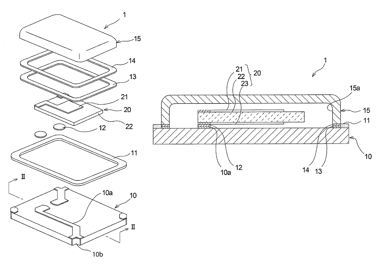
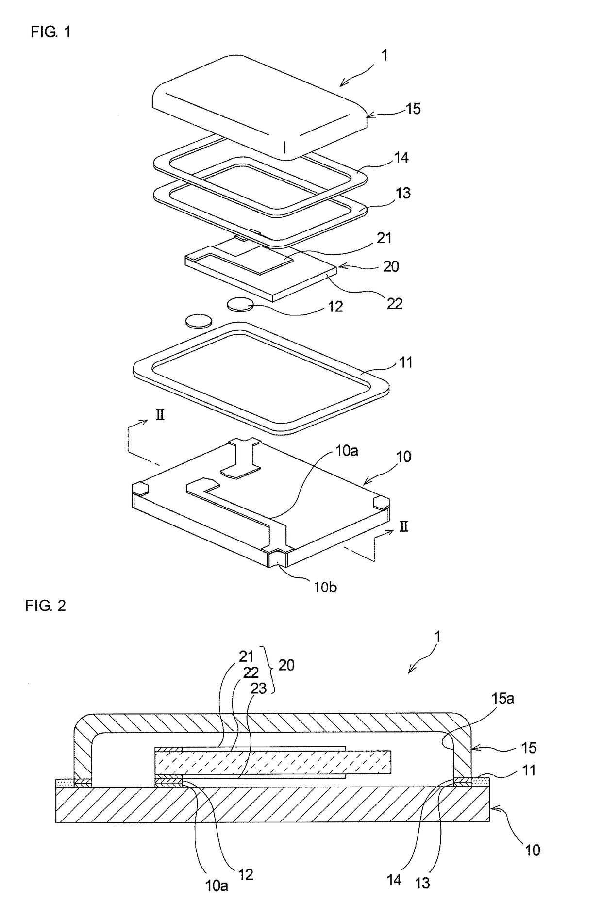
[0053]A piezoelectric vibration device having a structure substantially similar to that of the electronic component 1 illustrated in FIGS. 1 and 2 was manufactured in the following manner.

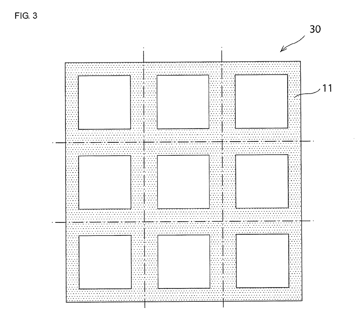
[0054]First, a motherboard formed of alumina was prepared as an original sealing member 30 illustrated in FIG. 3. Next, a frame-shaped glass layer having a thickness of 10 to 12 μm was formed by applying glass on a principal surface of the motherboard in a lattice form, as illustrated in FIG. 3. At this time, an area necessary to bond a below-described metal cap was left on the principal surface of the motherboard as a portion where the glass was not applied.

[0055]Next, the motherboard was cut to include the portion where the frame-shaped glass layer was applied, whereby an alumina substrate was formed as a first sealing member 10.

[0056]Next, a piezoelectric vibrator serving as an electronic component body 20 was mounted on the alumina substrate. Next, a metal cap formed of 42 nickel and serving as...


PUM

PropertyMeasurementUnit
thicknessaaaaaaaaaa
thicknessaaaaaaaaaa
timeaaaaaaaaaa

Abstract

A method for manufacturing an electronic component is provided where resin adhesive rarely spreads before curing. The method includes providing a first sealing member and forming a frame-shaped glass layer on a principal surface of the first sealing member. Moreover, the first sealing member is cut into multiple first sealing members and second sealing members are bonded with resin adhesive to inner frame regions on the principal surface of the first sealing member defined by the glass layer.

Description

CROSS REFERENCE TO RELATED APPLICATIONS[0001]The present application is a continuation of PCT / JP2012 / 052228 filed Feb. 1, 2012, which claims priority to Japanese Patent Application No. 2011-087379, filed Apr. 11, 2011, the entire contents of each of which are incorporated herein by reference.FIELD OF THE INVENTION[0002]The present invention relates to an electronic component having a sealed structure, and to a manufacturing method for the electronic component. More specifically, the present invention relates to an electronic component in which an electronic component body is provided in a sealed space, and to a manufacturing method for the electronic component.BACKGROUND OF THE INVENTION[0003]Various electronic components that require a sealed structure, for example, a piezoelectric vibration component including a piezoelectric vibration element, have hitherto been used. In such an electronic component having a sealed structure, the sealed structure is generally formed by bonding a ...

Claims


Application Information

Patent Timeline
Patent Type & Authority Patents(United States)
IPC IPC(8): H01L41/107H01L41/09H01L41/23H01L41/293H01L41/22H03H9/10H01L23/10H01L21/50H01L23/00H01L21/52H01L23/08H10N30/40H10N30/01H10N30/02H10N30/063H10N30/20
CPCH01L41/107H01L21/50H01L21/52H01L23/08H01L23/10H01L24/94H01L41/09H01L41/22H01L41/23H01L41/293H03H9/1021H01L2924/0002Y10T29/42Y10T29/4913Y10T29/49126Y10T29/49169Y10T156/1062H01L2924/0001H01L2924/00H10N30/40H10N30/01H10N30/02H10N30/20H10N30/063
Inventor OISHIBASHI, HIDEKAZUNAGAMINE, YUICHIROSATO, TAKEO
Owner MURATA MFG CO LTD
Learn More