Method of dividing wafer into dies

a technology of dies and wafers, applied in the direction of basic electric elements, electrical apparatus, semiconductor devices, etc., can solve the problems of large bending stress, unfavorable reuse, and damage to the devices formed on the wafer, so as to prevent the breakage of the wafer and/or the breakage of the cut, the effect of increasing processing quality and improving processing precision

Active Publication Date: 2017-07-11
DISCO CORP
View PDF32 Cites 0 Cited by
  • Summary
  • Abstract
  • Description
  • Claims
  • Application Information

AI Technical Summary

Benefits of technology

[0004]Accordingly, it is an object of the present invention to provide a method for dividing a wafer into dies that allows for an elimination of a die shift with low unit costs.

Problems solved by technology

In the process of peeling off a wafer from a carrier, the wafer is subjected to large bending stresses, which may result in breakage of the wafer and / or damage to the devices formed on the wafer.
Due to the bending of the wafer in the detachment process of the carrier, partially separated dies may touch each other and thus be damaged.
Further, large bending stresses also act on the carrier upon detachment thereof.
The carrier may thus be compromised or even broken in the removal process, rendering its reuse unfeasible.
For the reasons given above, the wafer has to be detached from the carrier very slowly and carefully, leading to a reduction in productivity, i.e., a reduced throughput of processed units per hour, and therefore increased processing costs.
The inventor has found that the drawbacks identified above are attributable to the fact that the carrier is glued to the adhesive tape over its whole surface area.
Accordingly, due to the large glued area, the detachment of the carrier from the wafer generates large bending stresses which are likely to cause damage to the wafer and / or the carrier.
Further, a treatment of the glued area for allowing a carrier detachment is likely to damage devices since the devices and the glued area are positioned above one another.
The result is a relatively high rejection rate, leading to high unit costs.

Method used


Image

  • Method of dividing wafer into dies
  • Method of dividing wafer into dies
  • Method of dividing wafer into dies

Examples


Embodiment Construction

[0030]A preferred embodiment of the present invention will now be described with reference to the accompanying drawings.

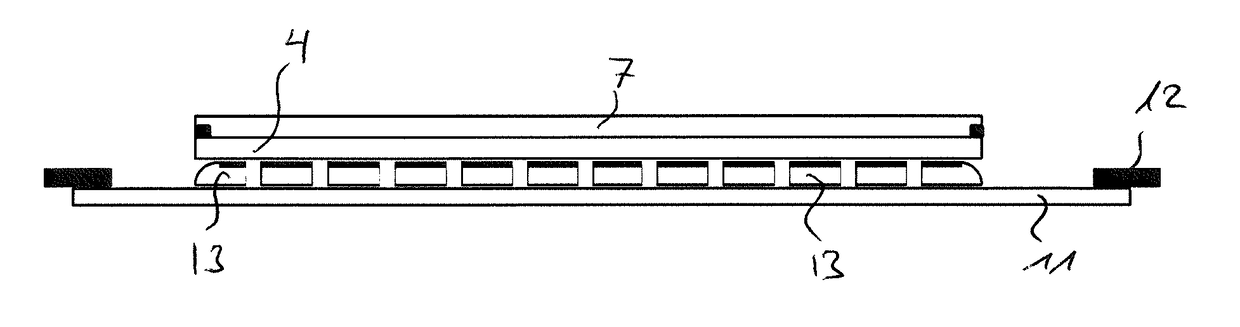
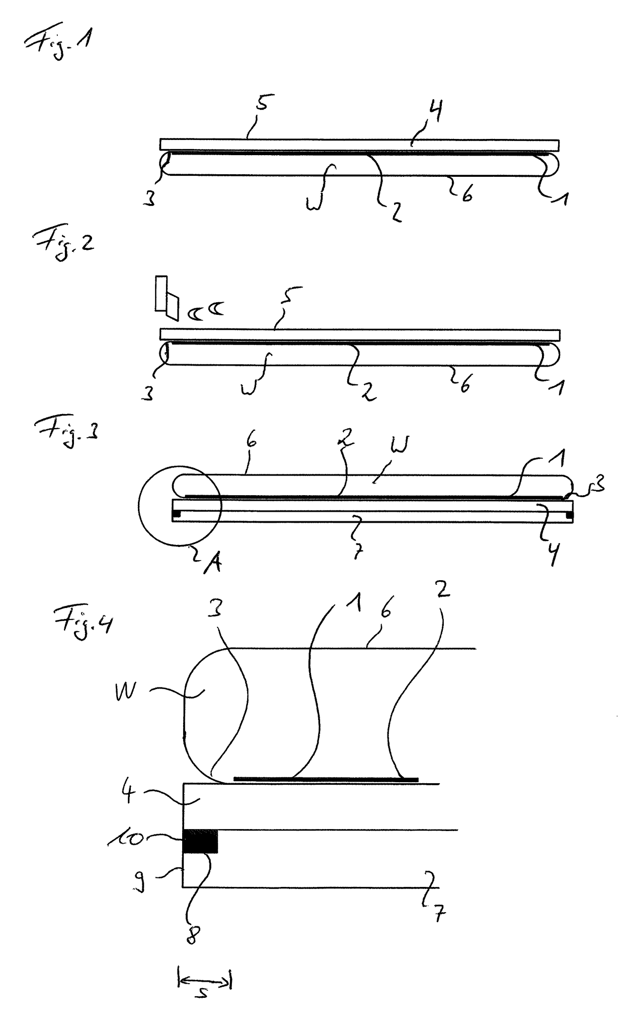
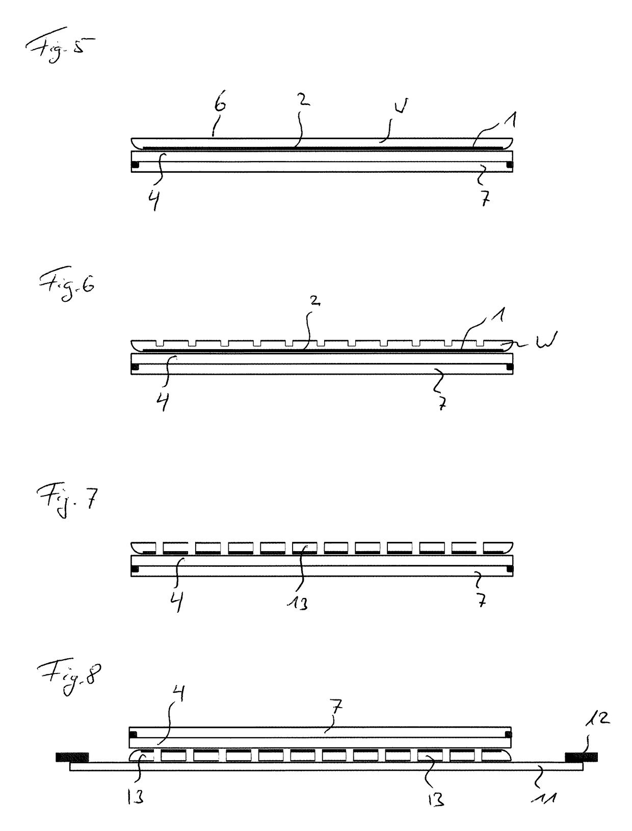
[0031]The following preferred embodiment relates to a method for dividing a wafer W into dies. The wafer W can be a MEMS wafer having MEMS devices formed on a side surface thereof, which is called a pattern side 1 in the following description. However, the wafer W is not limited to a MEMS wafer, but may also be a CMOS wafer having CMOS devices, preferably as solid-state imaging devices, formed on the pattern side 1 thereof. The wafer W can be made of silicon. Such a silicon wafer W can include devices as ICs (integrated circuits) and LSIs (large scale integrations) on a silicon substrate or may be an optical device wafer configured by forming optical devices such as LEDs (light emitting diodes) on an inorganic material substrate of ceramic, glass or sapphire. The wafer W is not limited to this and can be formed in any other way. Furthermore, also a combination of t...


PUM


Abstract

A method of dividing a wafer, having on one side a device area with a plurality of devices partitioned by a plurality of division lines and a peripheral marginal area with no devices formed around the device area, into dies is provided. The method comprises: attaching an adhesive tape for protecting devices on the wafer to the one side of the wafer, the adhesive tape adhering to at least some, optionally all, of the devices; connecting a carrier for supporting the adhesive tape to the side of the adhesive tape being opposite to the side in contact with the devices by connecting means; grinding that side of the wafer being opposite the one side for adjusting the wafer height; and cutting the wafer along the division lines. The method is characterized by locating the connecting means completely outward of the device area of the wafer in a top view thereon.

Description

TECHNICAL FIELD[0001]The present invention relates to a method of dividing a wafer, having on one side a device area with a plurality of devices partitioned by a plurality of division lines and a peripheral marginal area with no devices formed around the device area, into dies according to the preamble of claim 1.PRIOR ART[0002]In a semiconductor device fabrication process, a wafer having a device area with a plurality of devices partitioned by a plurality of division lines is divided into individual dies. This fabrication process generally comprises a grinding step of adjusting the wafer height and a cutting step of cutting the wafer along the division lines for obtaining the dies. To protect the devices formed on the wafer during this fabrication process and for positioning the individual dies, an adhesive tape can be attached to the wafer side having the devices formed thereon. However, this adhesive tape is easily deformable due to the drawback that, during the fabrication proce...

Claims


Application Information

Patent Timeline
Patent Type & Authority Patents(United States)
IPC IPC(8): H01L21/00H01L21/78H01L21/683H01L21/02
CPCH01L21/78H01L21/02013H01L21/6835H01L21/6836H01L2221/6834H01L2221/68318H01L2221/68327H01L2221/68381H01L2221/68386H01L21/67132
Inventor PRIEWASSER, KARL HEINZ
Owner DISCO CORP
Why Eureka
Try Eureka