Integrated circuits with non-volatile memory and methods of producing the same

a technology of integrated circuits and non-volatile memory, which is applied in the direction of electrical equipment, semiconductor devices, and testing/measurement of semiconductor/solid-state devices, etc., can solve the problems of reducing costs, increasing complexity, and increasing the size of memory cells with the rest of the microelectronic components

Inactive Publication Date: 2017-06-13
ALSEPHINA INNOVATIONS INC
View PDF1 Cites 0 Cited by
  • Summary
  • Abstract
  • Description
  • Claims
  • Application Information

AI Technical Summary

Benefits of technology

The patent describes methods and circuits for producing integrated circuits with a non-volatile memory cell. The methods involve forming a select layer over the memory area and the dummy area, and selectively etching a portion of the select layer to form a select gate in the memory area. The select etching is stopped when a certain concentration of indicator is measured. The methods also involve simultaneously removing a portion of the select layer from both the memory area and the dummy area to form a non-volatile memory cell with a control gate, a select gate, and a memory layer. The technical effects achieved by the patent text include improved methods for producing integrated circuits with a non-volatile memory cell, and increased efficiency and reliability of the memory cell.

Problems solved by technology

Market pressures are driving the industry to produce smaller components, but there is also significant market pressure to reduce costs while making smaller components.
There are numerous steps in the manufacture of many integrated circuits, and each step has an associated cost.
Many integrated circuits include memory cells to store information, and the memory cells are becoming smaller and more complex along with the rest of the microelectronic components.
The timed etch may not be as accurate or precise as an etch with an end point detection (e.g., an indicator gas that can be detected during the etch), but the relatively small area used for non-volatile memory in some integrated circuits does not produce sufficient indicator gases during the etch to detect the end point of the etch.
The timed etch can result in an inaccurate etch that may damage the substrate or leave a coating over the substrate that interferes with operation of the memory cells.

Method used


Image

  • Integrated circuits with non-volatile memory and methods of producing the same
  • Integrated circuits with non-volatile memory and methods of producing the same
  • Integrated circuits with non-volatile memory and methods of producing the same

Examples


Embodiment Construction

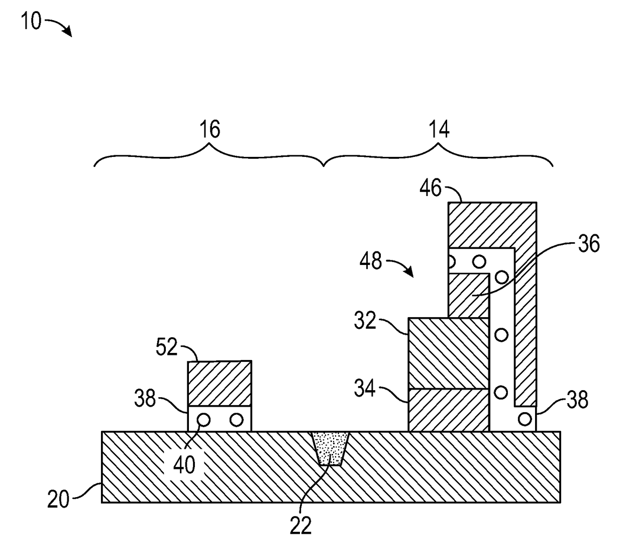
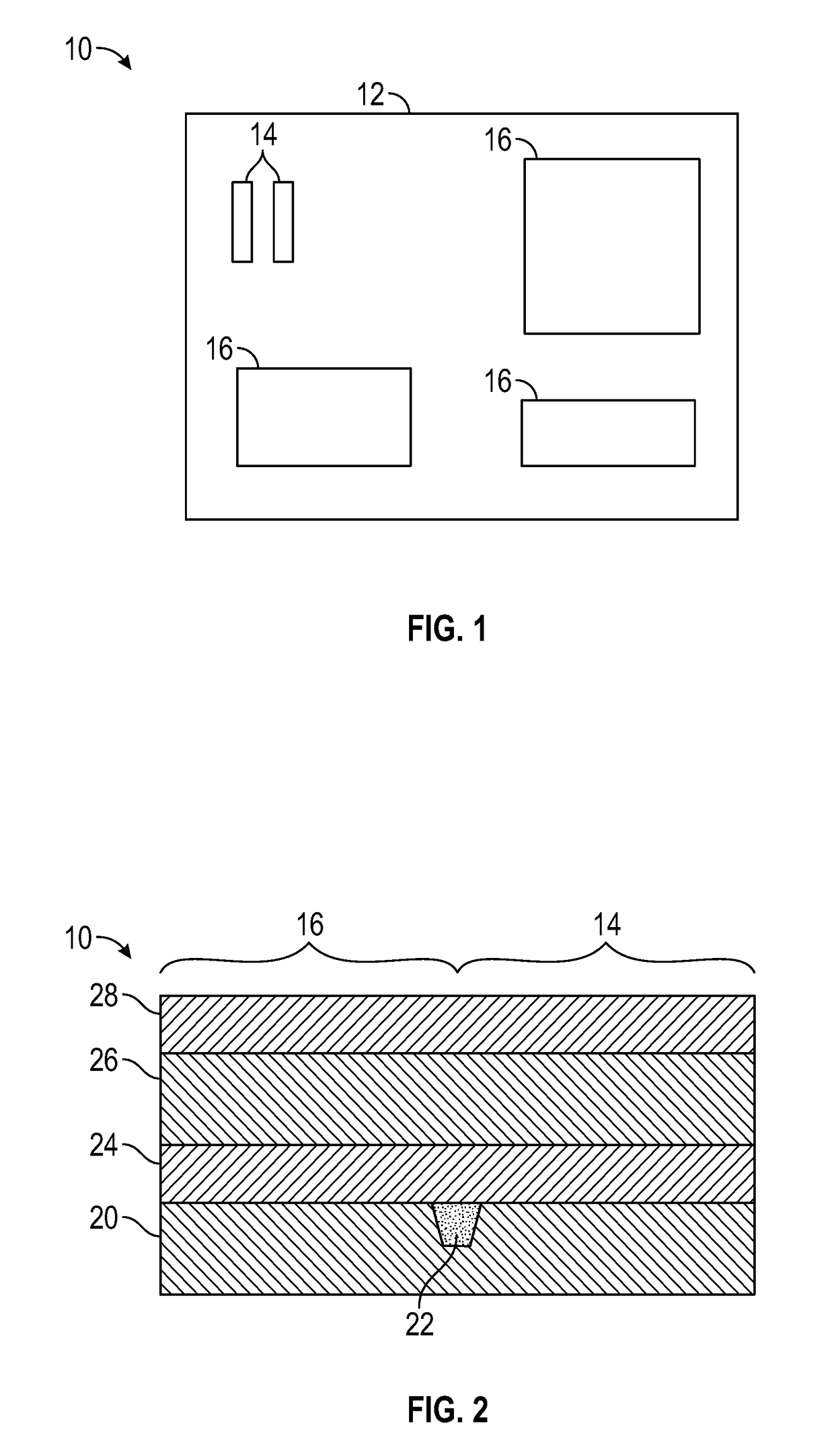
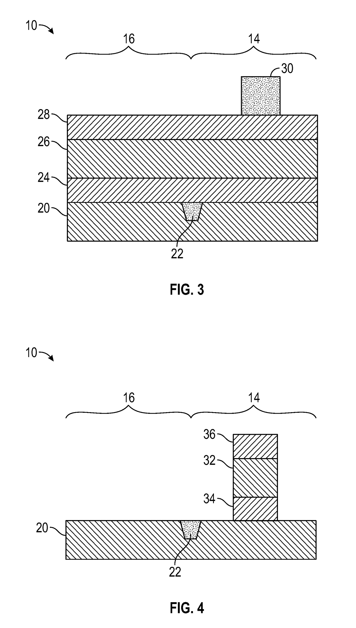
[0011]The following detailed description is merely exemplary in nature and is not intended to limit the various embodiments or the application and uses thereof. Furthermore, there is no intention to be bound by any theory presented in the preceding background or the following detailed description. Embodiments of the present disclosure are generally directed to integrated circuits and methods for fabricating the same. For the sake of brevity, conventional techniques related to integrated circuit device fabrication may not be described in detail herein. Moreover, the various tasks and process steps described herein may be incorporated into a more comprehensive procedure or process having additional steps or functionality not described in detail herein. In particular, various steps in the manufacture of semiconductor-based integrated circuits are well-known and so, in the interest of brevity, many conventional steps will only be mentioned briefly herein or will be omitted entirely with...


PUM


Abstract

Integrated circuits and methods of producing the same are provide. In an exemplary embodiment, a method includes determining a memory area of the integrated circuit, and forming a select layer overlying the substrate. A portion of the select layer is selectively etched to form a select gate within the memory area. A concentration of an indicator is measured in an etch off-gas during the selective etching of the select layer, and the selective etching of the select layer is terminated when the concentration of the indicator crosses an end point determination concentration.

Description

TECHNICAL FIELD[0001]The technical field generally relates to integrated circuits with non-volatile memory and methods of producing the same, and more particularly relates to integrated circuits with dummy gates and non-volatile memory, and methods of producing the same.BACKGROUND[0002]The semiconductor industry is continuously moving toward the fabrication of smaller and more complex microelectronic components with higher performance. Market pressures are driving the industry to produce smaller components, but there is also significant market pressure to reduce costs while making smaller components. There are numerous steps in the manufacture of many integrated circuits, and each step has an associated cost. Integrated circuits and methods of production that improve quality without requiring significant additional steps can reduce waste and improve reliability.[0003]Many integrated circuits include memory cells to store information, and the memory cells are becoming smaller and mor...

Claims


Application Information

Patent Timeline
IPC IPC(8): H01L21/28H01L21/66H01L27/1157H01L27/11582H01L27/11556H01L27/11524H01L27/11529H01L27/11573H01L27/11565H01L27/11519H01L21/3213H01L21/285H01L29/423H01L27/11
CPCH01L27/11556H01L27/11582H01L29/42332H01L29/42348H01L22/26H01L27/1157H01L27/11524H01L27/11529H01L27/11573H01L27/11565H01L27/11519H01L21/32136H01L21/28525H01L21/28556H01L21/31116H01L21/32137H01L29/42328H01L29/40114H10B41/43H10B43/40
Inventor LUO, LAIQIANGCHOW, YEW TUCK CLAMENTZHANG, FANLIU, HUAJUNWANG, DONGSHUM, DANNY PAK-CHUMTAN, JUAN BOON
Owner ALSEPHINA INNOVATIONS INC
Why Eureka
Try Eureka