
Three-dimensional image sensing device and method of sensing three-dimensional images

a three-dimensional image and sensing device technology, applied in the field of three-dimensional image sensing devices and a three-dimensional image sensing method, can solve the problems of increasing the cost of mobile devices and prior art not providing a proper integrated solution for users, and achieve the effects of gesture recognition, low cost and improved efficiency

Active Publication Date: 2017-05-30
EMINENT ELECTRONICS TECH
View PDF24 Cites 18 Cited by
  • Summary
  • Abstract
  • Description
  • Claims
  • Application Information

AI Technical Summary

Benefits of technology

The solution reduces costs and increases efficiency by canceling ambient visible light noise, enhancing depth sensing and gesture recognition capabilities while minimizing board space and power consumption.

Problems solved by technology

However, because two-dimensional image processors cannot determine depth of an image, gesture recognition capability of the two-dimensional image processors is significantly influenced.
For a mobile device, space of a printed circuit board for installing new components will significantly increase cost of the mobile device, so any mobile device has a requirement of integrating a combination of ambient visible light sensor, proximity sensor, color temperature sensor, and temperature sensor with gesture recognition into the same integrated circuit.
However, the prior art does not provide a proper integrated solution for a user.

Method used


Image

  • Three-dimensional image sensing device and method of sensing three-dimensional images
  • Three-dimensional image sensing device and method of sensing three-dimensional images
  • Three-dimensional image sensing device and method of sensing three-dimensional images

Examples


Embodiment Construction

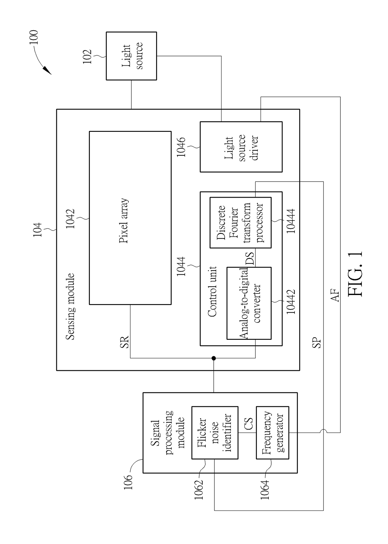
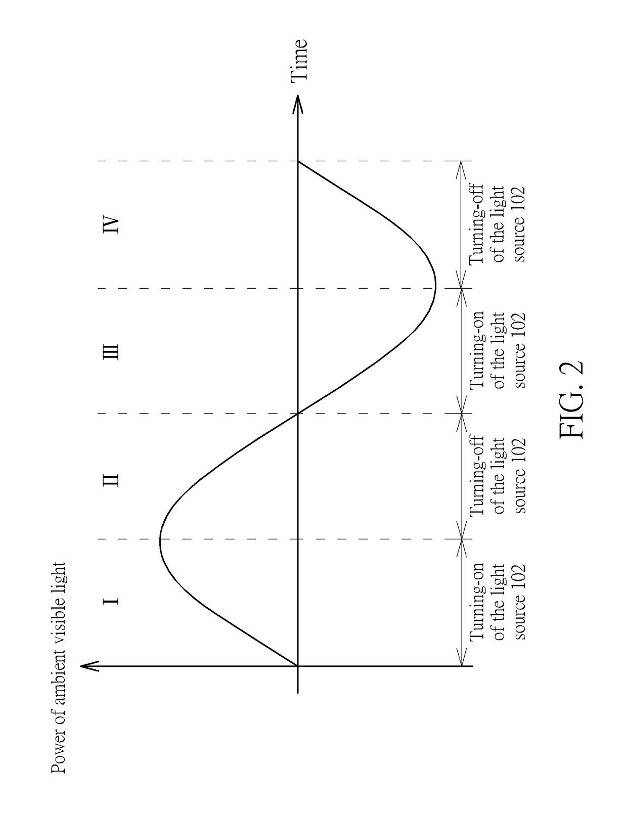
[0019]Please refer to FIG. 1. FIG. 1 is a diagram illustrating a three-dimensional image sensing device 100 according to an embodiment. As shown in FIG. 1, the three-dimensional image sensing device 100 includes a light source 102, a sensing module 104, and a signal processing module 106, wherein the sensing module 104 includes a pixel array 1042, a control unit 1044, and a light source driver 1046, and the control unit 1044 includes an analog-to-digital converter 10442 and a discrete Fourier transform processor 10444. The light source 102 can be an infrared ray (IR) light source or an IR laser light source (e.g. an IR light-emitting diode or an IR laser diode), and is used for generating flashing light with a K multiple of a frequency AF of flicker noise (wherein the frequency of the flicker noise can be equal to 100 Hz or 120 Hz) or a predetermined frequency, wherein exposure time of the pixel array 1042 during turning on of the light source 102 is equal to exposure time of the pi...


PUM


Abstract

A three-dimensional image sensing device includes a light source, a sensing module, and a signal processing module. The sensing module includes a pixel array, a control unit, and a light source driver. The light source generates flashing light with a K multiple of a frequency of flicker noise or a predetermined frequency. The pixel array samples the flashing light to generate a sampling result. The control unit executes an image processing on the sampling result to generate a spectrum. The light source driver drives the light source according to the K multiple of the frequency or the predetermined frequency. The signal processing module generates the K multiple of the frequency according to the spectrum, or outputs the predetermined frequency to the light source driver, and generates depth information according to a plurality of first images / a plurality of second images during turning-on / turning-off of the light source included in the sampling result.

Description

CROSS REFERENCE TO RELATED APPLICATIONS[0001]This application claims the benefit of U.S. Provisional Application No. 61 / 749,864, filed on Jan. 7, 2013 and entitled “3D gesture sensor architecture,” the contents of which are incorporated herein by reference.BACKGROUND OF THE INVENTION[0002]1. Field of the Invention[0003]The present invention relates to a three-dimensional image sensing device and a method of sensing three-dimensional images, and particularly to a three-dimensional image sensing device and a method of sensing three-dimensional images that can utilize an K multiple of a frequency of flicker noise or a predetermined frequency to cancel noise of ambient visible light.[0004]2. Description of the Prior Art[0005]With advance of human-device interfaces for mobile devices, the human-device interfaces have a trend toward nature user interfaces (NUIs), wherein gesture recognition is one of the most important NUI technologies, and various two-dimensional image processing can be ...

Claims


Application Information

Patent Timeline
Patent Type & Authority Patents(United States)
IPC IPC(8): H04N13/00G06K9/20G06F3/01G06K9/00H04N5/235G06F3/03G06V10/141G06V10/145
CPCH04N5/2357G06F3/017G06F3/0304G06K9/00355G06K9/2027G06K9/2036G06V40/28G06V10/145G06V10/141H04N23/745
Inventor CHANG, TOMWU, KAO-PINTSAI, KUN-HUANGHUNG, SHANG-MINGCHUANG, CHENG-TAFANG, CHIH-JENKUO-TSAI, TSENG
Owner EMINENT ELECTRONICS TECH
Learn More