
Liquid crystal display

a technology of liquid crystal display and display panel, which is applied in the direction of instruments, static indicating devices, etc., can solve the problems of difficult to achieve a narrow bezel design of the display panel, and the common voltage circuit of the display panel is more heavy

Active Publication Date: 2017-02-28
OPTRONIC SCI LLC
View PDF51 Cites 1 Cited by
  • Summary
  • Abstract
  • Description
  • Claims
  • Application Information

AI Technical Summary

Benefits of technology

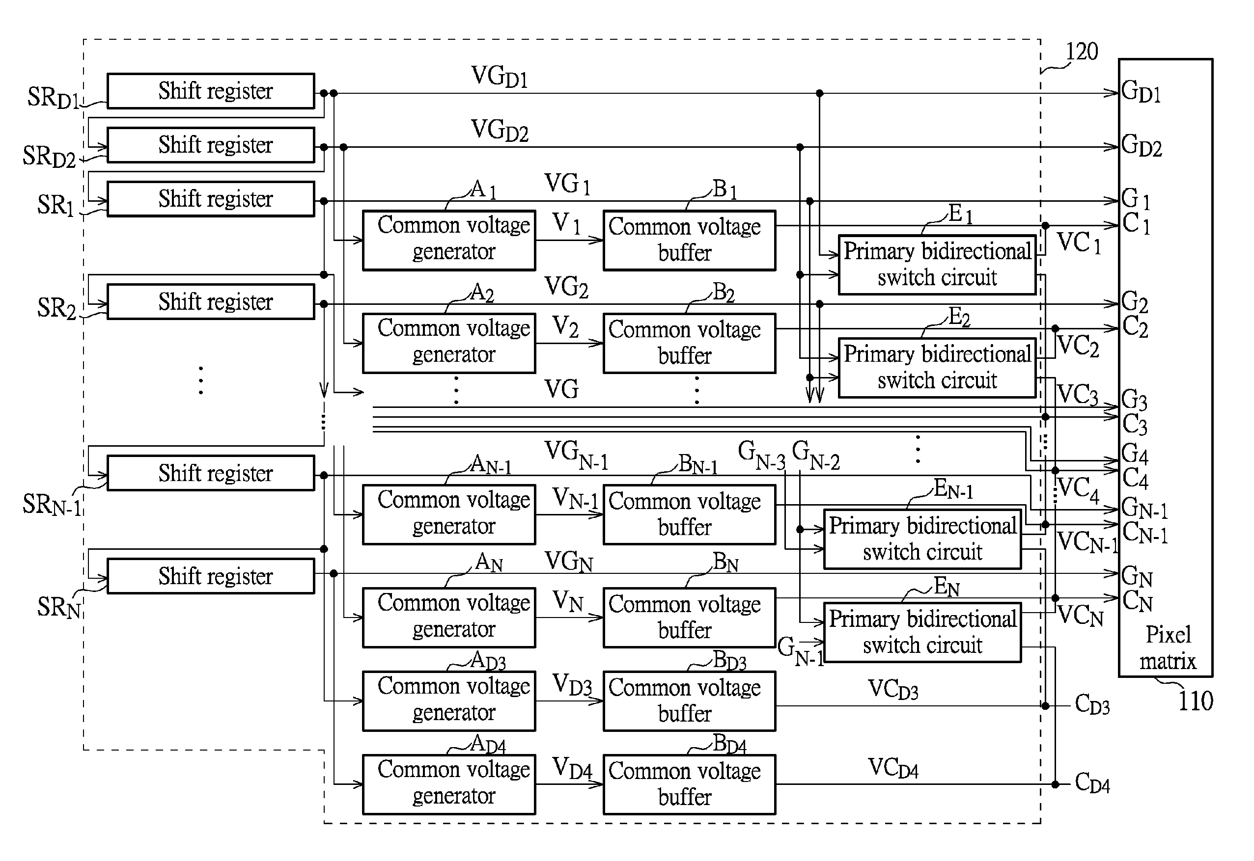
[0007]According to the embodiments of the present invention, with the help of primary bidirectional switch circuits, the LCD may control electrical connections of the common voltage lines according to timing of polarity inversion of each row of pixel. Accordingly, electric charge of each common voltage line may be shared to other common voltage lines, and an equivalent capacitance of pixels driven by the common voltage buffers may be not too great. Since the equivalent capacitance of pixels driven by the common voltage buffers may be not too great, the layout area of the common voltage buffers may be reduced to contribute to the achievement of a narrow bezel design of the display panel.

Problems solved by technology

However, high resolution results in a greater load of the common voltage circuits of the display panel, such that it is required to increase the size of common voltage buffers of the display panel to improve the current driving capability thereof for feeding a greater load.
Since large-sized common voltage buffers require a greater layout area, it is difficult to achieve a narrow bezel design of the display panel.

Method used


Image

  • Liquid crystal display
  • Liquid crystal display
  • Liquid crystal display

Examples


Embodiment Construction

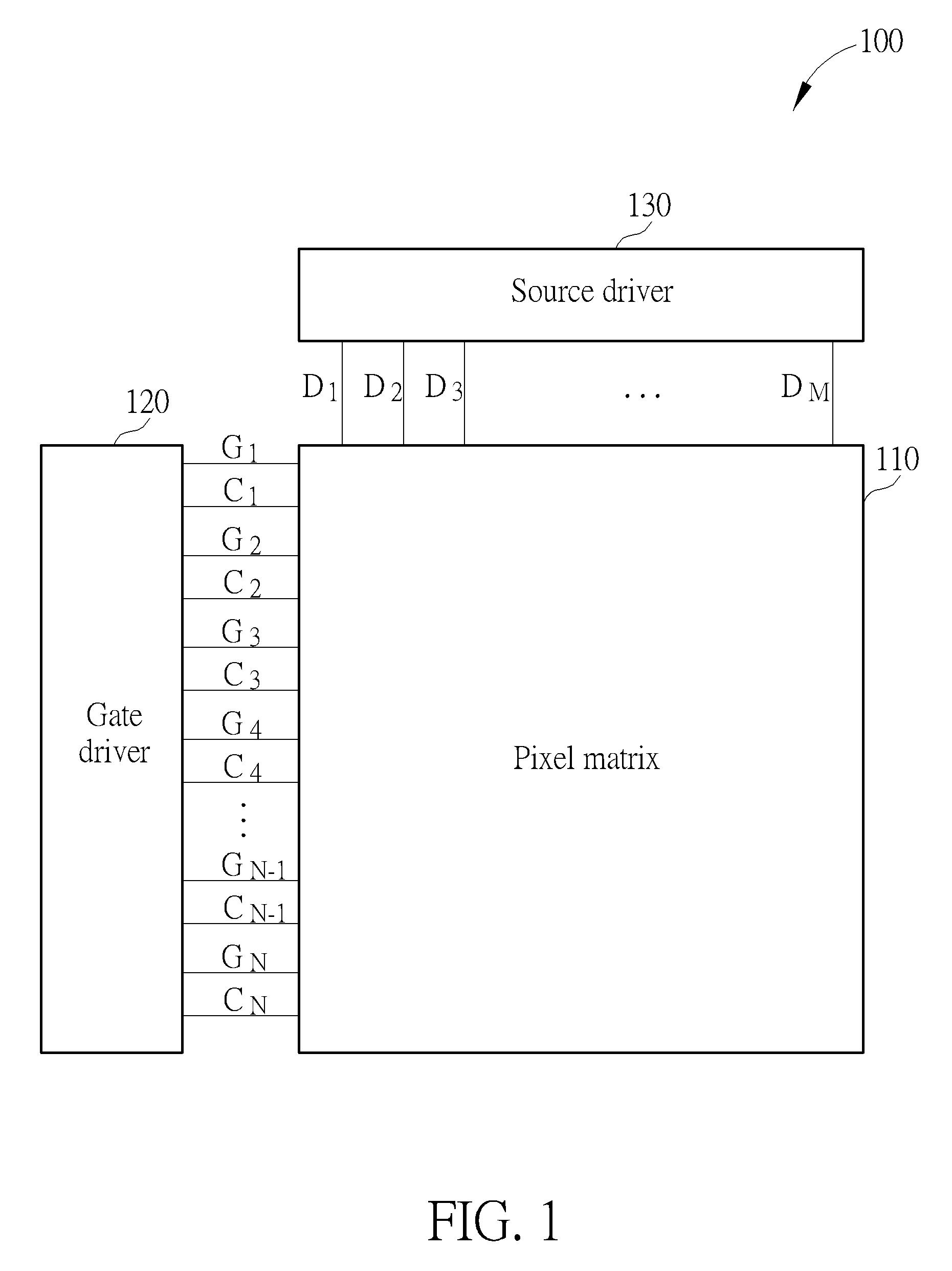
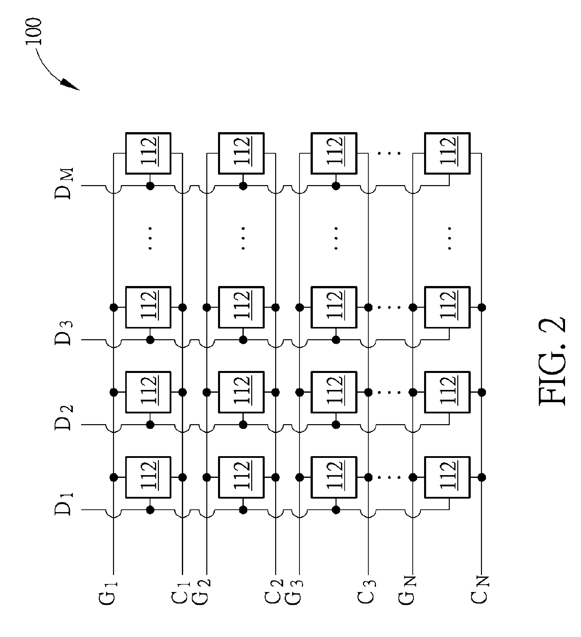
[0028]Please refer to FIGS. 1 to 3. FIG. 1 is a schematic diagram of a liquid crystal display 100 according to an embodiment of the present invention. FIG. 2 is a schematic diagram of a pixel matrix 110 in FIG. 1. FIG. 3 is a circuit diagram of a pixel 112 in FIG. 2. The liquid crystal display 100 comprises the pixel matrix 110, a gate driver 120 and a source driver 130. The pixel matrix 110 comprises a plurality of pixels 112, a plurality of scan lines G1 to GN, a plurality of common voltage lines C1 to CN and a plurality of data lines D1 and DM. The pixels 112 are arranged in N rows and M columns, where M and N are positive integers. Each of the scan lines G1 to GN is coupled to the pixels 112 arranged in one of the rows, and each of the common voltage lines C1 to CN is coupled to the pixels 112 arranged in one of the rows. Each of the pixels 112 has a switch SW, a storage capacitor Cst and a liquid crystal capacitor Clc. The switch SW may be a thin film transistor (TFT). Each of ...


PUM


Abstract

A liquid crystal display (LCD) has a pixel matrix, a plurality of shift registers, a plurality of common voltage generators, a plurality of common voltage buffers, and a plurality of primary bidirectional switch circuits. The shift registers sequentially output gate signals to scan lines of the pixel matrix. The common voltage generators output initial common voltages according to the gate signals. The common voltage buffers are configured to buffer the initial common voltages to output a plurality of common voltages to a plurality of common voltage lines of the pixel matrix. Each of the primary bidirectional switch circuits is configured to control electrical connection between two of the common voltage lines according to one or more gate signals outputted from at least one of the shift registers.

Description

BACKGROUND OF THE INVENTION[0001]1. Field of the Invention[0002]The present invention is related to a liquid crystal display, and more particularly to a liquid crystal display capable of sharing electric charge of common voltage lines thereof.[0003]2. Description of the Prior Art[0004]Liquid crystal displays (LCDs) are the most popular displays nowadays. Due to the properties of lightweight, low energy consumption, and free of radiation emission, LCDs have gradually replaced the cathode ray tube (CRT) monitors of conventional personal computers and have been widely-used in many portable information products, such as notebooks, personal digital assistants (PDAs), etc.[0005]Due to the vigorous development of smart phones, customer demand for small-sized display panels with a narrow bezel and high resolution design is increasing. However, high resolution results in a greater load of the common voltage circuits of the display panel, such that it is required to increase the size of commo...

Claims


Application Information

Patent Timeline
Patent Type & Authority Patents(United States)
IPC IPC(8): G09G3/18G09G3/36
CPCG09G3/3677G09G3/3614G09G3/3655G09G3/3611G09G3/3648G09G2300/0809G09G2310/0286G09G2310/0291
Inventor WU, MING-HUNG
Owner OPTRONIC SCI LLC
Learn More