Organic electroluminescence element and lighting device using same
a technology of electroluminescence elements and lighting devices, applied in the direction of basic electric elements, semiconductor devices, electrical equipment, etc., can solve the problems of reducing the efficiency of light propagation to the outside in which light emission is observed, and 70 to 80 % of the total amount of produced light does not effectively contribute to light emission, etc., to achieve enhanced light-outcoupling efficiency, reduced view angle dependence, and increased efficiency of light emerging outside
- Summary
- Abstract
- Description
- Claims
- Application Information
AI Technical Summary
Benefits of technology
Problems solved by technology
Method used
Image
Examples
second embodiment
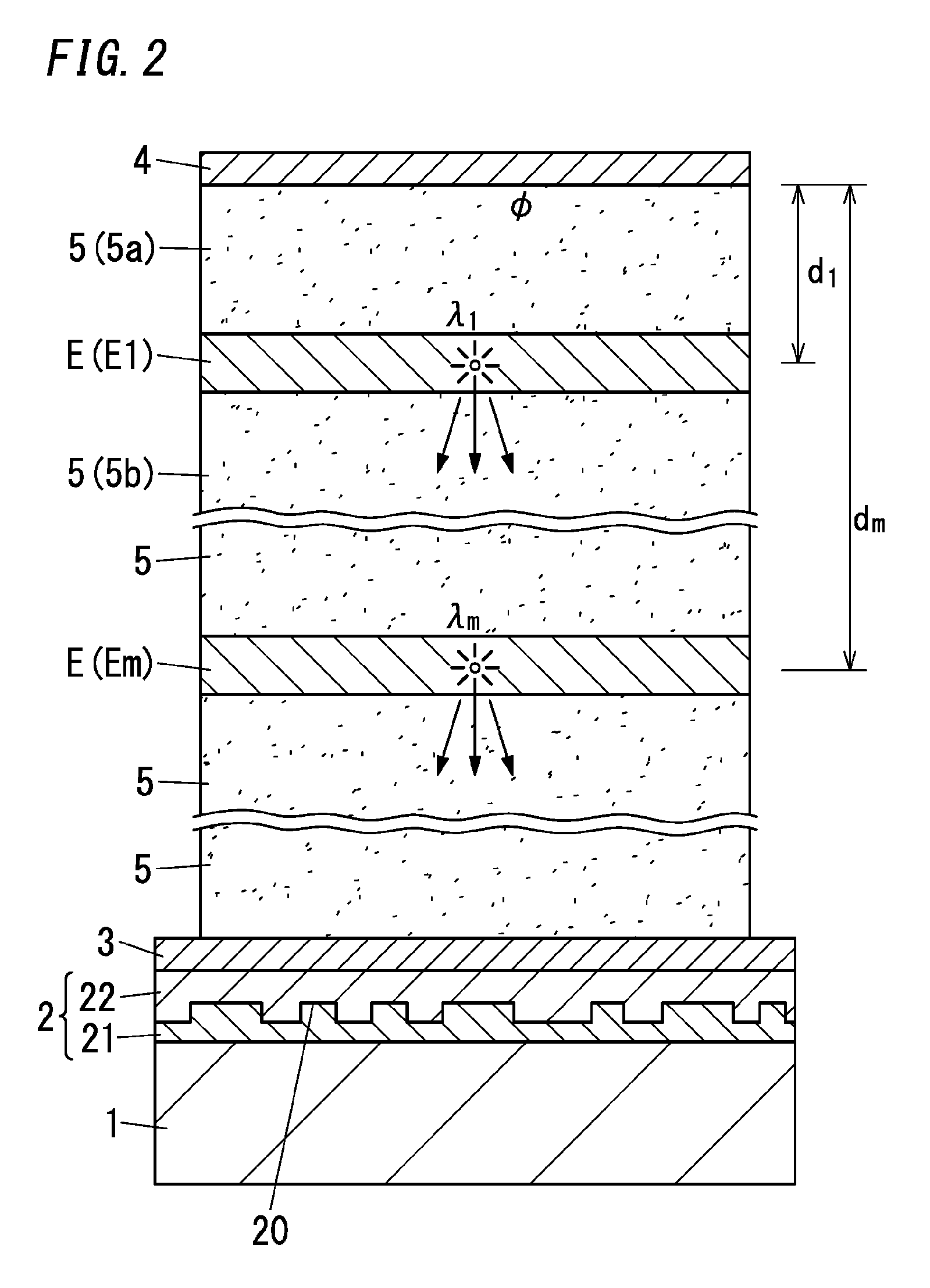
[0062]The present invention is explained with reference to the second embodiment whose reference signs relating to light emitting layers E are expressed by use of general expressions. Note that, the following explanation may be also applied to each embodiment.
[0063]In the present description, the light emitting layers E includes the m-th closest light emitting layer E to the light reflective electrode 4, which is referred to as an m-th light emitting layer Em. In this regard, m is an integer equal to or more than 1. For example, the first closest light emitting layer E to the light reflective electrode 4 is referred to as a first light emitting layer E1. Additionally, the second closest light emitting layer E to the light reflective electrode 4 is referred to as a second light emitting layer E2.
[0064]λm represents a weighted average emission wavelength of the m-th light emitting layer Em. For example, a weighted average emission wavelength of the first light emitting layer E1 is rep...
third embodiment
[0091]In the third embodiment, the light-outcoupling layer 7 is provided to the opposite surface of the substrate 1 from the light diffusion layer 2. When the light-outcoupling layer 7 is provided, total reflection at an interface between the substrate 1 and an outside (atmosphere) can be suppressed, and an amount of light emerging outside can be increased.
[0092]Note that, a distance from the light emitting layer E to a surface of the light transmissive electrode 3 facing the substrate 1 is represented by D. The reference point of the position of the light emitting layer E for determining the distance D may be same as that for determining the distance d, and may be the center of the light emitting layer E in the thickness direction thereof.
[Design of Element]
[0093]With reference to a design model of the organic EL element, it is explained that the aforementioned relations are preferable.
[0094]FIG. 4 shows the design model of the organic EL element. This design model is used to optim...
first embodiment
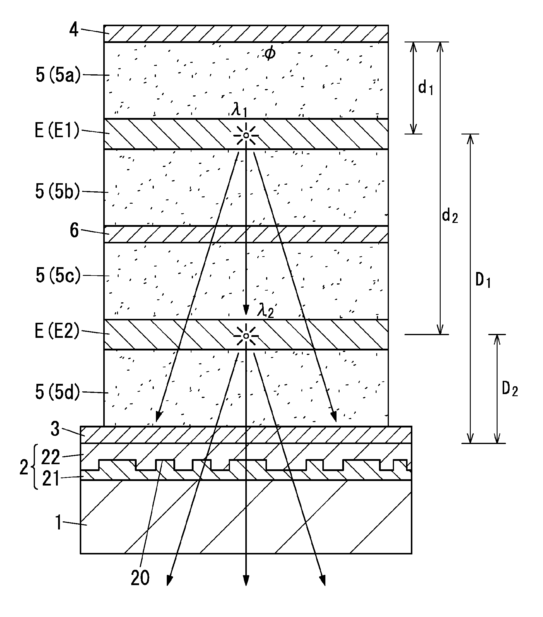
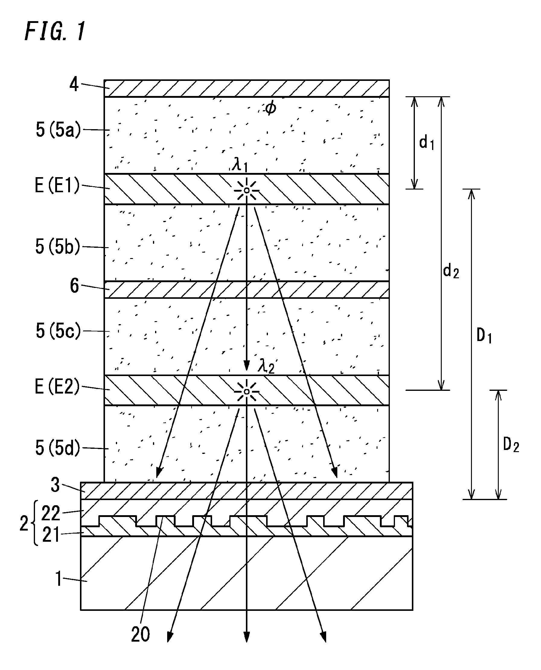
[0104]First, the organic EL element with the multi-unit structure was prepared, experimentally. This prototype has the same layer structure as the first embodiment illustrated in FIG. 1. The whole emission color of this is white. The white emission is important for the lighting use and the like. The first light emitting layer E1 has the weighted average emission wavelength (λ1) of 600 nm. The emission color of the first light emitting layer E1 is orange. The second light emitting layer E2 has the weighted average emission wavelength (λ2) of 470 nm. The emission color of the second light emitting layer E2 is blue. The medium filling the space between the first light emitting layer E1 and the light reflective electrode 4 has the average refractive index (n) of 1.80, and the extinction coefficient (k) of 0.0005. These refractive index and extinction coefficient are averages with regard to the wavelength λ1. The medium filling the space between the second light emitting layer E2 and the...
PUM
 Abstract
Description
Claims
Application Information
 - R&D
- Intellectual Property
- Life Sciences
- Materials
- Tech Scout
- Unparalleled Data Quality
- Higher Quality Content
- 60% Fewer Hallucinations
Browse by: Latest US Patents, China's latest patents, Technical Efficacy Thesaurus, Application Domain, Technology Topic, Popular Technical Reports.
© 2025 PatSnap. All rights reserved.Legal|Privacy policy|Modern Slavery Act Transparency Statement|Sitemap|About US| Contact US: help@patsnap.com


